Eureka AIR delivers breakthrough ideas for toughest innovation challenges, trusted by R&D personnel around the world.

A grid line electrode structure on the back surface of a monocrystalline silicon solar cell and a monocrystalline silicon solar cell

A solar cell and back surface technology, which is applied in the field of solar cells, can solve the problems of large amount of silver paste usage and large backside recombination, and achieve the effects of reducing usage, reducing backside recombination, and improving photoelectric conversion efficiency

Active Publication Date: 2016-11-16
江苏润阳世纪光伏科技有限公司
View PDF4 Cites 0 Cited by
  • Summary
  • Abstract
  • Description
  • Claims
  • Application Information

AI Technical Summary

Problems solved by technology

At present, in this method, the emitter fine grid electrode is a thicker (compared to the back field fine grid electrode) grid line. Although the series resistance is small, the amount of silver paste used is large, and the rear side is recombined.

Method used


Image

  • A grid line electrode structure on the back surface of a monocrystalline silicon solar cell and a monocrystalline silicon solar cell
  • A grid line electrode structure on the back surface of a monocrystalline silicon solar cell and a monocrystalline silicon solar cell
  • A grid line electrode structure on the back surface of a monocrystalline silicon solar cell and a monocrystalline silicon solar cell

Examples


Embodiment 1

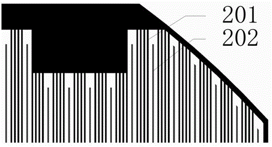
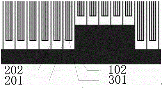
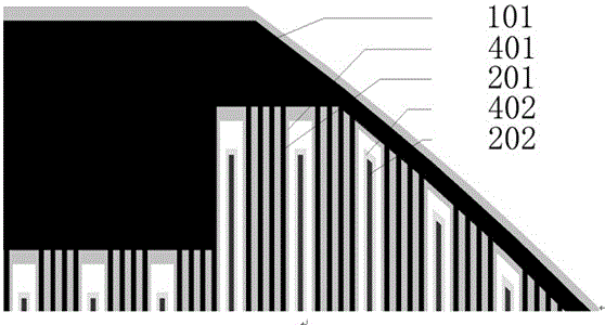
[0030] Such as Figure 1-4 As shown in , the grid line electrode structure on the back surface of the monocrystalline silicon solar cell provided in this embodiment uses a silicon wafer of 156 mm×156 mm with rounded chamfered n-type single crystal silicon wafers, including The p-type emitter 401 and the n-type back field 402 on the surface, the p-type emitter 401 and the n-type back field 402 are alternately distributed and not in contact with each other, and also include the p-type emitter main gate electrode 101, the n-type back field main gate The electrode 102, the p-type emitter fine grid electrode 201 and the n-type back field fine grid electrode 202, wherein the p-type emitter fine grid electrode 201 is located on the p-type emitter 401, and the n-type back field fine grid electrode 202 is located on the n-type back surface On the field 402, the p-type emitter fine grid electrode 201 is connected to the p-type emitter main gate electrode 101, the n-type back field fine ...

Embodiment 2

[0039] Such as Figure 5 As shown in a, the gate line electrode structure on the back surface of the monocrystalline silicon solar cell provided in this embodiment adopts a 4 mm×4 mm square n-type single crystal silicon wafer, including The p-type emitter and the n-type back field, the p-type emitter and the n-type back field are distributed alternately and do not touch each other, and also include the p-type emitter main gate electrode, the n-type back field main gate electrode, the p-type emitter fine The gate electrode and the n-type back field fine grid electrode, wherein the p-type emitter fine grid electrode is located on the p-type emitter, the n-type back field fine grid electrode is located on the n-type back field, and the p-type emitter fine grid electrode is connected to the p-type The emitter main grid electrode is connected, the n-type back field fine grid electrode is connected to the n-type back field main grid electrode, and each p-type emitter fine grid elect...

Embodiment 3

[0051] The difference from Embodiment 1 is that in this implementation, each p-type emitter fine grid electrode is composed of five parallel and evenly distributed thin grids, and the ends of the five parallel and uniformly distributed thin grids are connected by a thin grid.


PUM


Abstract

The invention discloses a grid line electrode structure on the back surface of a monocrystalline silicon solar cell, which comprises a p-type emitter and an n-type back field arranged on the back surface of a single-crystal silicon wafer, and the p-type emitter and the n-type back field are alternately distributed And not in contact with each other, it also includes p-type emitter main grid electrode, n-type back field main grid electrode, p-type emitter fine grid electrode and n-type back field fine grid electrode, the p-type emitter fine grid electrode is located on the p-type emitter On the pole, the n-type back field fine grid electrode is located on the n-type back field, the p-type emitter fine grid electrode is connected to the p-type emitter main grid electrode, and the n-type back field fine grid electrode is connected to the n-type back field main grid electrode Each p-type emitter fine grid electrode is composed of a plurality of parallel and evenly distributed fine grids, and the ends of the parallel and uniformly distributed fine grids are connected by a fine grid, and the grid line electrode structure with the above-mentioned back surface is also disclosed Back-junction and back-contact solar cells, which can reduce the amount of silver paste used and recombine on the back, and improve photoelectric conversion efficiency.

Description

technical field [0001] The invention belongs to the field of solar cells, and in particular relates to a grid line electrode structure on the back surface of a single crystal silicon solar cell and the single crystal silicon solar cell. Background technique [0002] With the rapid increase of energy consumption and increasingly serious environmental pollution, solar energy has developed rapidly as a renewable clean energy source. The main way to utilize solar energy is photovoltaic power generation, and the core device of photovoltaic power generation is solar cells. [0003] At present, commercial solar cells are mainly based on crystalline silicon solar cells, including single crystal silicon and polycrystalline silicon, and most of them are p-type substrates. With the advancement of technology and the reduction of cost, high-efficiency monocrystalline silicon solar cells made of n-type monocrystalline silicon with better performance have shown good application prospects a...

Claims


Application Information

Patent Timeline
Patent Type & Authority Patents(China)
IPC IPC(8): H01L31/0224H01L31/068
CPCH01L31/022433H01L31/022441H01L31/0682Y02E10/547
Inventor 沈辉姜辰明李力王殿磊
Owner 江苏润阳世纪光伏科技有限公司
Why Eureka
Eureka Blog
Learn More