Copper reduction process for printed circuit board

A printed circuit board and process technology, applied in the field of printed circuit board manufacturing technology, can solve problems such as failure of hole copper etching to meet control requirements

Inactive Publication Date: 2014-11-05
东莞市五株电子科技有限公司
View PDF4 Cites 16 Cited by
  • Summary
  • Abstract
  • Description
  • Claims
  • Application Information

AI Technical Summary

Problems solved by technology

[0003] The technical problem mainly solved by the present invention is that in the production process...

Method used


Image

  • Copper reduction process for printed circuit board
  • Copper reduction process for printed circuit board
  • Copper reduction process for printed circuit board

Examples


Embodiment Construction

[0022] The following will clearly and completely describe the technical solutions in the embodiments of the present invention. Obviously, the described embodiments are only some of the embodiments of the present invention, rather than all the embodiments. Based on the embodiments of the present invention, all other embodiments obtained by persons of ordinary skill in the art without making creative efforts belong to the protection scope of the present invention.

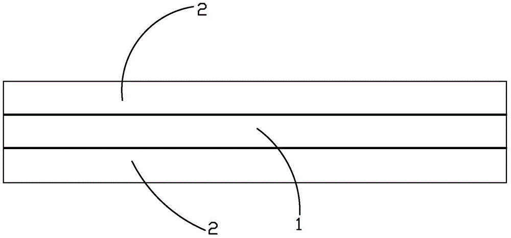
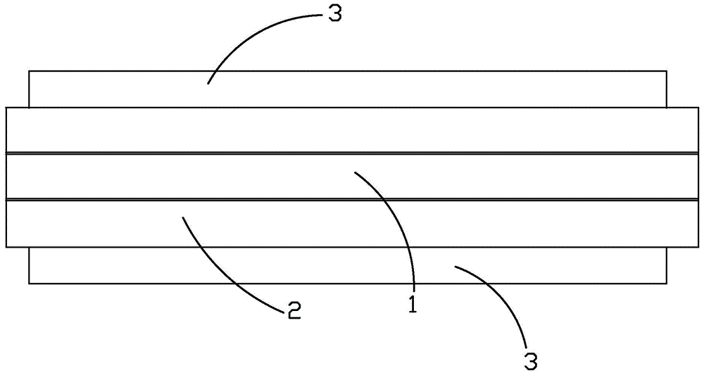
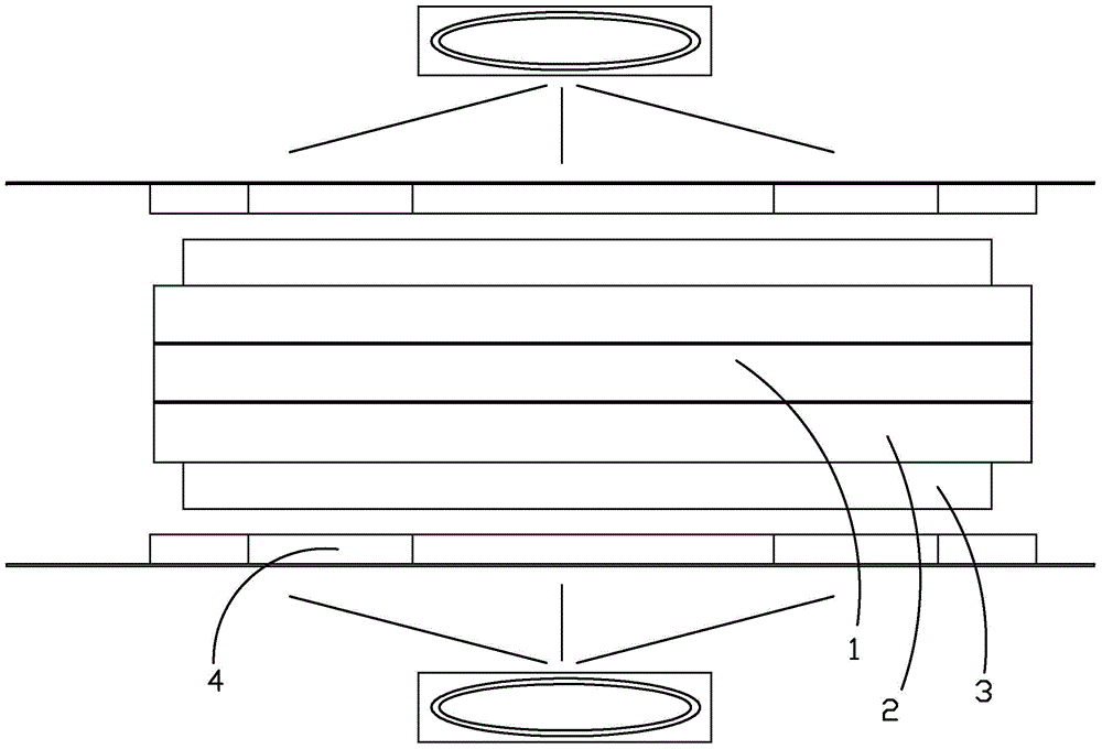
[0023] see Figure 1 to Figure 6 , the embodiment of the present invention discloses a copper reduction process for a printed circuit board, the copper reduction process for a printed circuit board includes the following steps:

[0024] Pressed dry film: the substrate after the whole board is copper-plated (such as figure 1 shown) to carry out the dry film pressing process, the dry film 3 is pressed on the upper and lower sides of the substrate, and the hole ring on the substrate is covered by the dry film 3, as f...


PUM


Abstract

The invention provides a copper reduction process for a printed circuit board. The copper reduction process comprises: a dry film pressing step in which the processing of dry film pressing is performed on an integrally copper-plated substrate, and dry films are pressed on upper and lower surfaces of the substrate, wherein and a pore ring on the substrate is covered with the dry films; an exposing step in which the dry films on the two surfaces of the substrate are exposed, a part of the dry film not to be needed is irradiated by the light with a present wavelength; a developing step in which the exposed dry films are developed, and the part of the dry film not to be needed is removed; a copper reducing step in which unneeded surface copper on the developed substrate is removed, wherein as the pore ring is covered with the dry films, and a chemical reaction does not occur between copper reducing solution and the dry films, pore copper is not reduced; a film removing step in which the dry films on the substrate subjected to the copper reducing are completely removed; and a board grinding step in which grinding is performed so that the height of a copper layer at the pore ring and the height of the surface copper are consistent. In the copper reduction process for the printed circuit board, since the dry films cover the pore ring before the copper reducing step, an acid etching solution cannot chemically react with the dry films in the copper reducing step, so that pore copper is protected, reliability of the thickness of the pore copper is further guaranteed, and copper is ingeniously reduced.

Description

technical field [0001] The invention relates to a process for manufacturing a printed circuit board (PCB), in particular to a copper reduction process for a printed circuit board. Background technique [0002] In the production process of printed circuit boards, in order to meet the requirements of surface copper thickness control, the general practice is to perform copper reduction treatment after copper electroplating. For example, the thickness of copper on the electroplating surface is 70um (bottom copper 17, electroplating copper 20*3=60um), and the copper needs to be reduced to 20-25um to ensure that 2mil lines can be made. The thickness of the copper in the through-hole of the circuit board is generally required to be 25um. The industry usually directly reduces the copper wire after electroplating. The copper on the surface of the printed circuit board and the copper in the hole are etched by the copper wire reduction solution at the same time. Thickness (20-25um) re...

Claims


Application Information

Patent Timeline
IPC IPC(8): H05K3/22
Inventor 孟昭光
Owner 东莞市五株电子科技有限公司
Why Eureka
Try Eureka