Method and device for generating PCB manufacturing sheet information

A technology for generating units and single boards, applied in special data processing applications, instruments, electrical digital data processing, etc., can solve problems such as spending a lot of time and energy, affecting PCB design and production, and prolonging the occupied time, so as to avoid omissions, The effect of saving a lot of time consumption

Inactive Publication Date: 2014-12-03
INSPUR BEIJING ELECTRONICS INFORMATION IND
View PDF6 Cites 5 Cited by
  • Summary
  • Abstract
  • Description
  • Claims
  • Application Information

AI Technical Summary

Problems solved by technology

[0004] The method of manually inputting the requirements in the PCB design involved in the design and making the production order information requires a lot of time and energy on the one hand; informa

Method used


Image

  • Method and device for generating PCB manufacturing sheet information
  • Method and device for generating PCB manufacturing sheet information

Examples


Embodiment Construction

[0032] In order to make the purpose, technical solution and advantages of the application clearer, the embodiments of the application will be described in detail below in conjunction with the accompanying drawings. It should be noted that, in the case of no conflict, the embodiments in the present application and the features in the embodiments can be combined arbitrarily with each other.

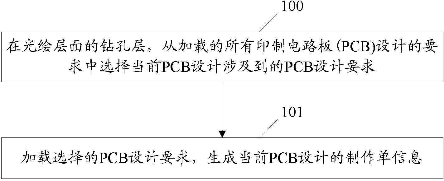
[0033] figure 1 The flow chart of the method for generating PCB manufacturing single information for the present invention, as figure 1 shown, including:

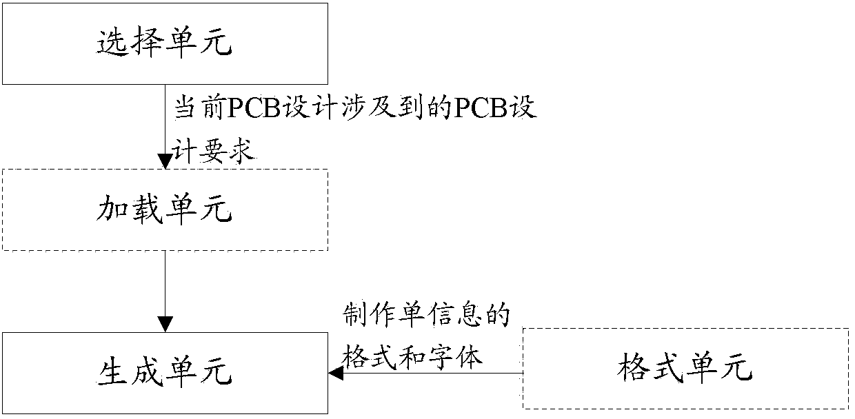
[0034] Step 100 , in the drilling layer of the gerberography layer, select the PCB design requirements involved in the current PCB design from all loaded PCB design requirements.

[0035] It should be noted that the selection here refers to setting the corresponding selection key by setting each PCB design requirement, such as the selection control in software design. When the selection control is confirmed as confirmed, the correspond...


PUM


Abstract

The invention discloses a method and a device for generating PCB manufacturing sheet information. The method includes: on the drilling layer of a light painting layer, selecting PCB design requirements related to current PCB design from all loaded PCB (printed circuit board) design requirements; loading the selected PCB design requirements to generate the manufacturing sheet information of current PCB design. By the arrangement, the method has the advantages that a large amount of time consumed in manual input during manufacturing sheet information manufacturing, and manufacturing sheet information missing caused by manual input is avoided.

Description

technical field [0001] The present application relates to printed circuit board technology, in particular to a method and device for generating printed circuit board (PCB) manufacturing information. Background technique [0002] At present, in the design and processing of printed circuit boards (PCB), the requirements for PCB processing are getting higher and higher. In addition, as the signal rate of PCB transmission continues to increase, the requirements for board materials, impedance requirements, and acceptance standards in PCB design are becoming more and more stringent. If the production of the PCB cannot meet the standards set at the time of design, for example, the PCB (BGA) area of ​​the ball grid array structure has not been completed and needs to be plugged, or the thickness of the board does not exceed the thickness of the gold finger as required, etc., processed out The PCB is just unusable. [0003] In order to produce PCB products that meet the standards, t...

Claims


Application Information

Patent Timeline
IPC IPC(8): G06F17/50
Inventor 赵亚民李鹏翀
Owner INSPUR BEIJING ELECTRONICS INFORMATION IND
Why Eureka
Try Eureka