

Capacitance type fingerprint sensor packaging structure and packaging method
A fingerprint sensor and packaging structure technology, which is applied in the field of biometric module packaging, can solve the problems of large surface area and large substrate area, and achieve the effect of reducing surface area and facilitating miniaturization
- Summary
- Abstract
- Description
- Claims
- Application Information
AI Technical Summary
Problems solved by technology
Method used
Image

Examples
Embodiment Construction
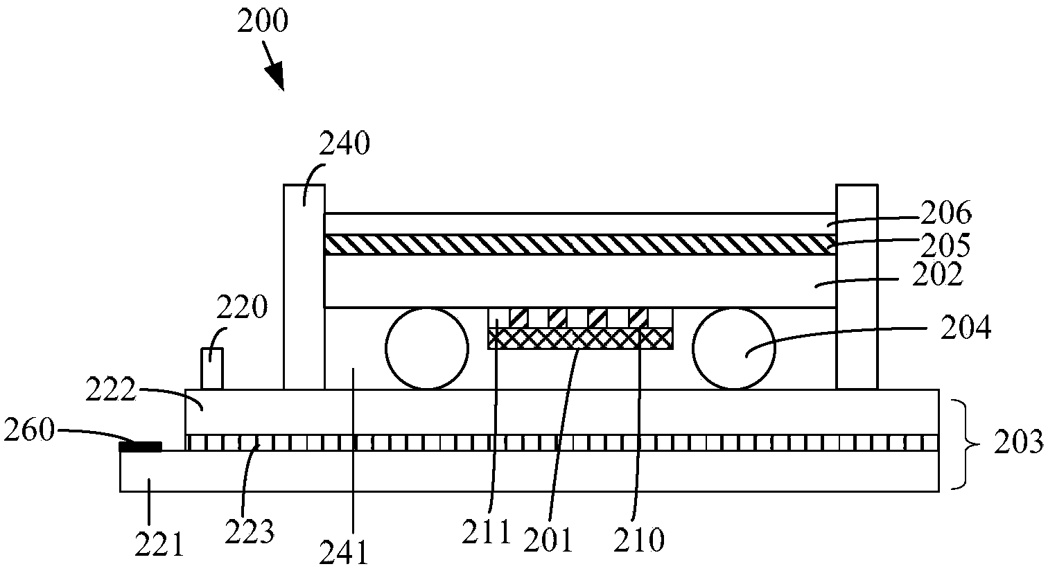
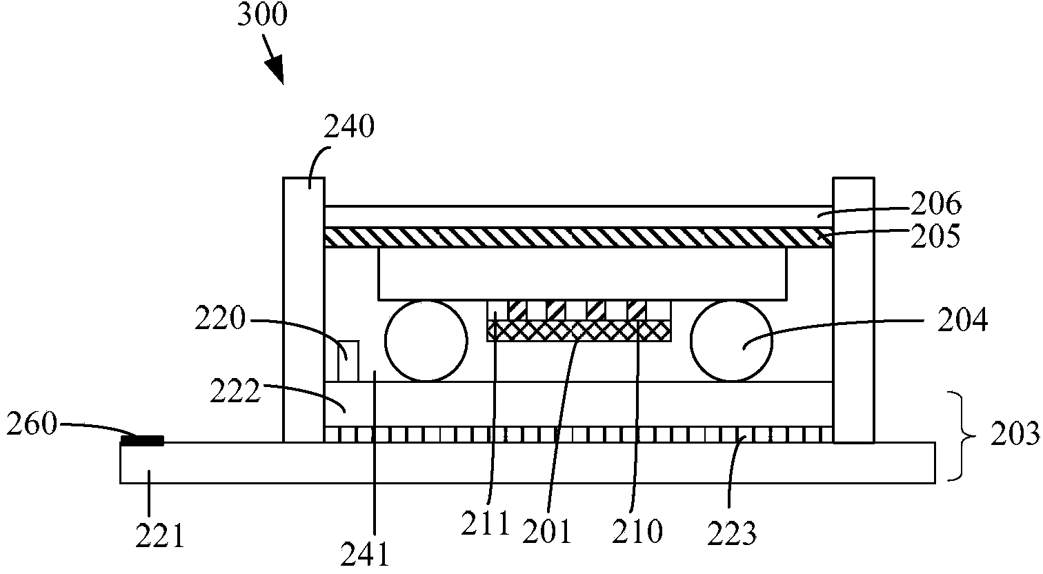
[0026] This embodiment provides a capacitive fingerprint sensor packaging structure, and the capacitive fingerprint sensor packaging structure can be specifically arranged in a fingerprint identification device. The fingerprint identification device is used to identify the user's fingerprint.
[0027] Such as Figure 1A Shown is a schematic diagram of the package structure of the capacitive fingerprint sensor according to this embodiment. The capacitive fingerprint sensor packaging structure 200 includes an independently packaged chip 201 , a fingerprint sensing element 202 and a substrate 203 .
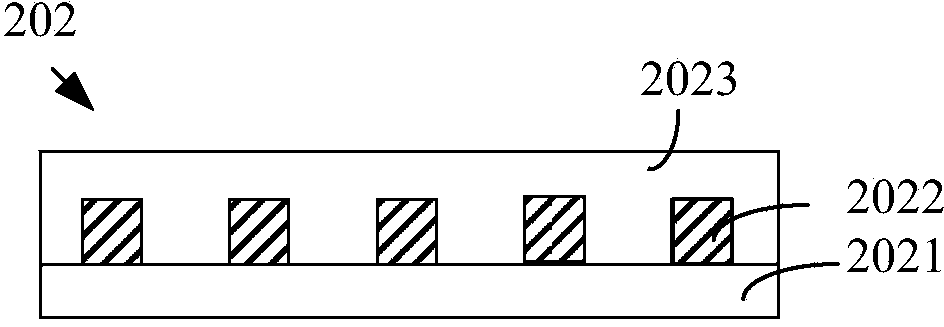
[0028] Among them, the fingerprint sensing element 202 is arranged above the chip 201 and is electrically connected with the chip 201. Specifically, the chip 201 and the fingerprint sensing element 202 can be electrically connected in a flip-chip manner; the substrate 203 is arranged below the chip 201, and the substrate 203 and the fingerprint sensing element 202 is electrically co...
PUM
| Property | Measurement | Unit |
|---|---|---|
| Thickness | aaaaa | aaaaa |
| Thickness | aaaaa | aaaaa |
| Flatness | aaaaa | aaaaa |
Abstract
Description
Claims
Application Information