Method for preparing transmission electron microscopy (TEM) sample

A sample and preparation technology, which is applied in the field of preparing TEM samples, can solve the problems of insufficient uniformity, imperfection, and laboriousness of ion beams, and achieve the effects of ensuring quality, saving machines, and high quality

Active Publication Date: 2014-12-10
WUHAN XINXIN SEMICON MFG CO LTD
View PDF3 Cites 8 Cited by
  • Summary
  • Abstract
  • Description
  • Claims
  • Application Information

AI Technical Summary

Problems solved by technology

However, for the preparation of ultra-high-height samples that need to take pictures of multi-layer structures with a thickness of more than 3 microns, it is necessary to roughly dig a large deep pit from the chip surface to form a marking pit, and the subsequent thinning cannot be less than 2 µm. The digging depth is twice as much as the preparation of general TEM samples, and the whole process will be very laborious and time-consuming
Moreover, the prepared samples are often not perfect due to insufficient uniformity of the ion beam, which is undesirable for those skilled in the art

Method used


Image

  • Method for preparing transmission electron microscopy (TEM) sample
  • Method for preparing transmission electron microscopy (TEM) sample
  • Method for preparing transmission electron microscopy (TEM) sample

Examples


Embodiment Construction

[0036] The present invention will be further described below in conjunction with the accompanying drawings and specific embodiments, but not as a limitation of the present invention.

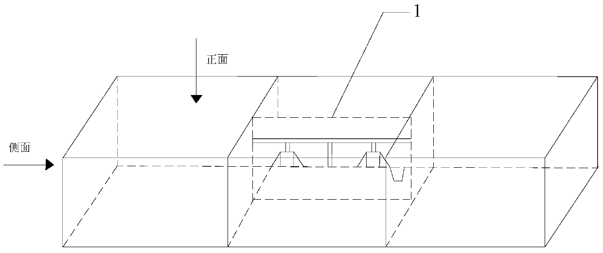
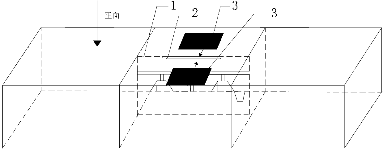
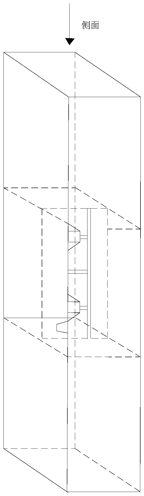
[0037] For the structure to be tested that needs to be photographed with a multi-layer structure and the thickness reaches 3 μm or more, a large pit is roughly excavated from the front of the structure to be tested to form a marking pit, and continue to thin. Therefore, the present invention provides a method for preparing TEM samples, focusing on rapid grinding from the side to the point of failure and then cutting the sample with a knife. Since the point of failure or the required structure is rotated, the depth is at most 2 μm, so The time for preparing samples using this invention will be equal to the conventional preparation time, thereby greatly saving the machine, time and labor costs. In addition, using the method of the present invention, the failure point of the failed chip and the corr...


PUM

PropertyMeasurementUnit
thicknessaaaaaaaaaa
thicknessaaaaaaaaaa
depthaaaaaaaaaa

Abstract

The invention relates to the technical field of semiconductor manufacturing, and in particular relates to a method for preparing a transmission electron microscopy (TEM) sample. The method comprises the steps of acquiring the position of a failure point of a failure chip and the position of a failure analysis reference point of a non-failure chip, polishing the failure chip to the part near the failure point along the direction vertical to a selected side, and polishing the non-failure chip to the part near the failure analysis reference point along the direction vertical to the selected side; sticking the front of the failure chip and the front of the non-failure chip together to form a structure to be tested; and putting the structure to be tested into a focused ion beam (FIB) machine with the polished surface being upward to prepare the TEM sample. Therefore, the TEM sample can be rapidly prepared; the most appropriate thickness can be found out when a picture with high resolution is shot, so that the quality of the picture with high resolution can be guaranteed.

Description

technical field [0001] The invention relates to the technical field of semiconductor manufacturing, in particular to a method for preparing TEM samples. Background technique [0002] At present, transmission electron microscopy (TEM) is an important tool in electron microscopy, and TEM can be used to detect the morphology, size and characteristics of thin films that make up semiconductor devices. After the TEM sample is placed in the TEM observation room, the main working principle of the TEM is: when the high-energy electron beam penetrates the TEM sample, phenomena such as scattering, absorption, interference, and diffraction occur, so that a contrast is formed on the imaging plane, thereby forming an image of the TEM sample , followed by observation, measurement and analysis of the image of the TEM sample. [0003] In the prior art, the focused ion beam (FIB) machine can complete the preparation of TEM samples in a local area of ​​the entire wafer. In the process of usin...

Claims


Application Information

Patent Timeline
Patent Type & Authority Applications(China)
IPC IPC(8): G01N1/28G01N1/32
Inventor 高慧敏张顺勇
Owner WUHAN XINXIN SEMICON MFG CO LTD
Why Eureka
Try Eureka