

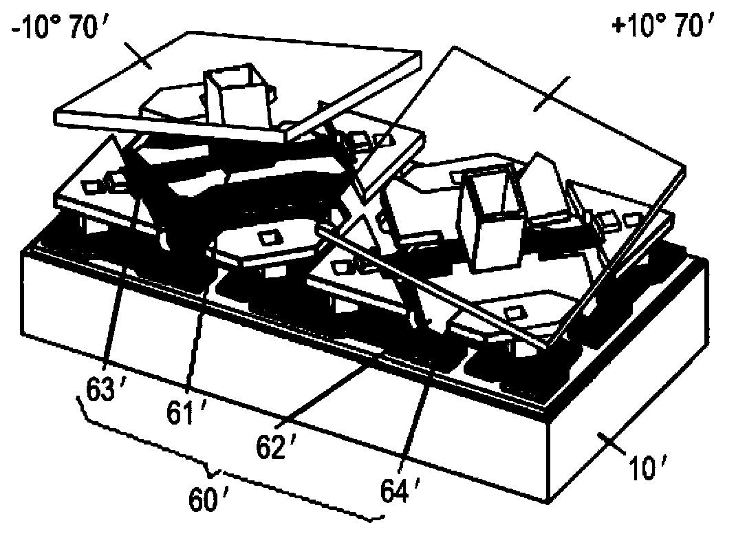
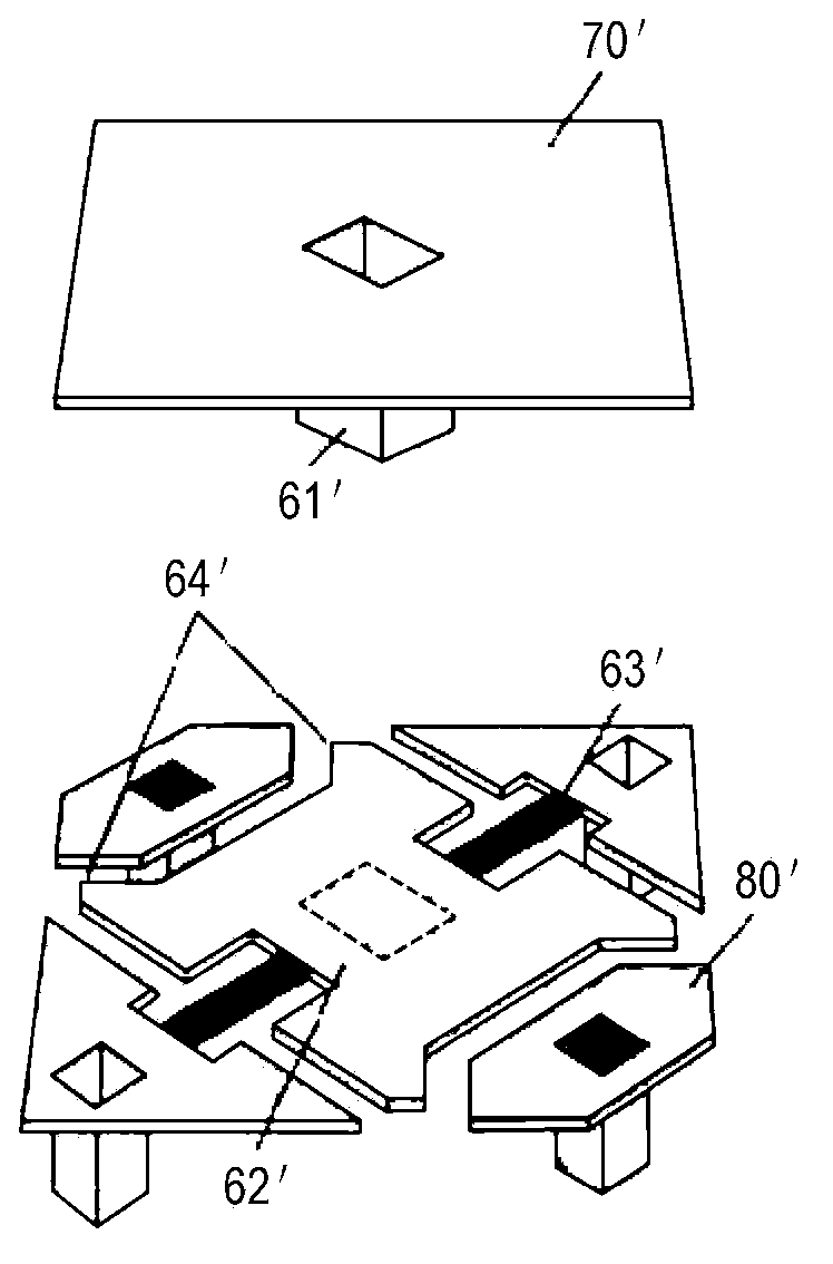
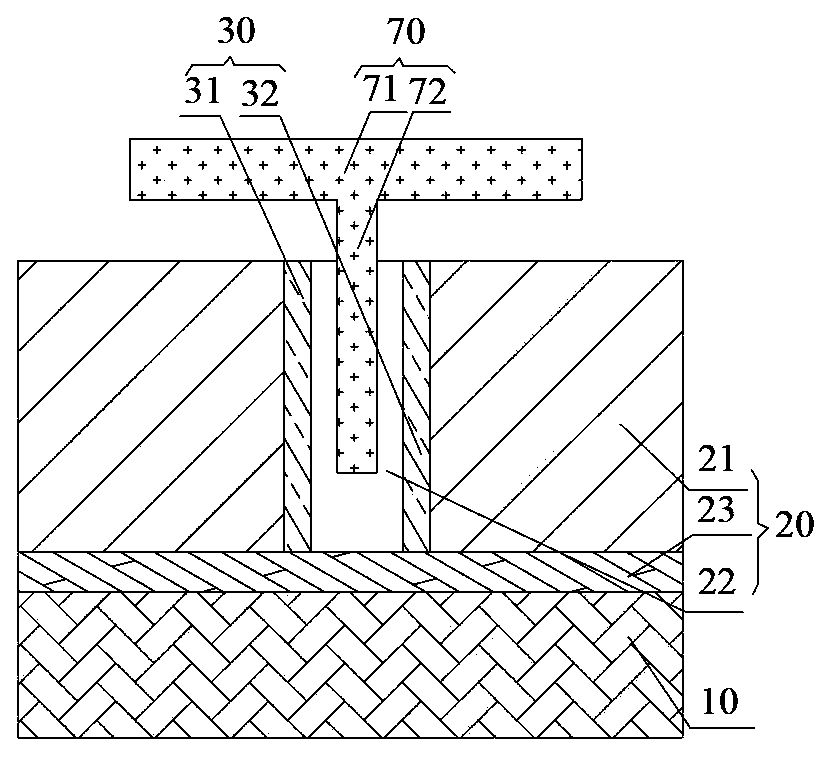
Single-pixel structure, digital micro-mirror device with same and production method of single-pixel structure and digital micro-mirror device
A single-pixel, support structure technology, applied in the direction of instruments, optical components, optics, etc., can solve the problems of complex structure, not too small lens size, low yield rate, etc.
- Summary
- Abstract
- Description
- Claims
- Application Information
AI Technical Summary
Problems solved by technology
Method used
Image

Examples
Embodiment Construction
[0043] It should be pointed out that the following detailed description is exemplary and intended to provide further explanation to the present application. Unless defined otherwise, all technical and scientific terms used herein have the same meaning as commonly understood by one of ordinary skill in the art to which this application belongs.
[0044] It should be noted that the terms used here are only used to describe specific embodiments, and are not intended to limit the exemplary embodiments according to the present application. As used herein, unless the context clearly indicates otherwise, the singular form is also intended to include the plural form. In addition, it should also be understood that when the terms "comprising" and / or "comprising" are used in this specification, it indicates There are features, steps, operations, means, components and / or combinations thereof.
[0045] For ease of description, spatially relative terms, such as "on," "over," "above," etc.,...
PUM
 Abstract
Description
Claims
Application Information