Array substrate, manufacturing method thereof and display device

A technology of an array substrate and a manufacturing method, which is applied in the field of liquid crystal display, can solve the problems affecting the light efficiency of the display panel, the display effect of the display panel, and the transmittance of the display panel, etc., so as to achieve the effect of improving the display quality and eliminating the phenomenon of dark areas.

Active Publication Date: 2014-12-17
BOE TECH GRP CO LTD +1
View PDF5 Cites 3 Cited by
  • Summary
  • Abstract
  • Description
  • Claims
  • Application Information

AI Technical Summary

Problems solved by technology

like figure 1 As shown, the common electrode pattern includes a plurality of hollowed out areas S, the width of the hollowed out area S is d, and the length is not greater than the length of a pixel area. The area M in the figure is the area where the common electrode and the pixel electrode overlap. In the hollowed out area S The area inside the dotted line frame at the lower end will form a dark area due to the disorder of liquid crystal orientation, which will seriously affect the transmittance of the display panel and affect the display of the display panel; at the same time, when the display panel is working, the electric field formed by the gate electrode will often affect the deflection of the liquid crystal. , causing light leakage in the area near the gate electrode. In order for the common electrode to block the light leakage, the end of the hollowed out region S needs to maintain a distance of at least a from the gate electrode, so that the position of the dark area formed at the end of the hollowed out region S in the pixel area It will be relatively high, which will further affect the light effect of the display panel

Method used


Image

  • Array substrate, manufacturing method thereof and display device
  • Array substrate, manufacturing method thereof and display device
  • Array substrate, manufacturing method thereof and display device

Examples


Embodiment 1

[0066] In this embodiment, a conductive pattern is formed above the gate electrode, so that the projection of the gate electrode in a direction perpendicular to the base substrate falls into the conductive pattern. Specifically, the manufacturing method of the array substrate of this embodiment includes the following steps:

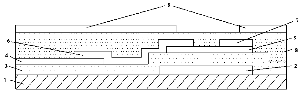
[0067] In step a1: provide a base substrate 1, and form patterns of gate electrodes 2 and gate lines on the base substrate 1;

[0068] A base substrate 1 is provided, on which a pattern consisting of a gate metal layer including a gate electrode 2 and a gate line connected to the gate electrode 2 is formed. Wherein, the base substrate 1 may be a glass substrate or a quartz substrate.

[0069] Specifically, sputtering or thermal evaporation can be used to deposit a layer with a thickness of The gate metal layer, the gate metal layer can be Cu, Al, Ag, Mo, Cr, Nd, Ni, Mn, Ti, Ta, W and other metals and alloys of these metals, the gate metal layer can be s...

Embodiment 2

[0090] In this embodiment, a conductive pattern is formed above the gate electrode, so that the projection of the gate electrode in a direction perpendicular to the substrate falls into the conductive pattern, and the conductive pattern is connected to the source electrode or the drain electrode through a via hole. Specifically, the manufacturing method of the array substrate of this embodiment includes the following steps:

[0091] In step b1: provide a base substrate 1, and form patterns of gate electrodes 2 and gate lines on the base substrate 1;

[0092] A base substrate 1 is provided, on which a pattern consisting of a gate metal layer including a gate electrode 2 and a gate line connected to the gate electrode 2 is formed. Wherein, the base substrate 1 may be a glass substrate or a quartz substrate.

[0093] Specifically, sputtering or thermal evaporation can be used to deposit a layer with a thickness of The gate metal layer, the gate metal layer can be Cu, Al, Ag, M...

Embodiment 3

[0114] In this embodiment, a conductive pattern is formed above the gate electrode, so that the projection of the gate electrode in a direction perpendicular to the base substrate falls into the conductive pattern. Specifically, the manufacturing method of the array substrate of this embodiment includes the following steps:

[0115] In step c1: provide a base substrate 1, and form patterns of gate electrodes 2 and gate lines on the base substrate 1;

[0116] A base substrate 1 is provided, on which a pattern consisting of a gate metal layer including a gate electrode 2 and a gate line connected to the gate electrode 2 is formed. Wherein, the base substrate 1 may be a glass substrate or a quartz substrate.

[0117] Specifically, sputtering or thermal evaporation can be used to deposit a layer with a thickness of The gate metal layer, the gate metal layer can be Cu, Al, Ag, Mo, Cr, Nd, Ni, Mn, Ti, Ta, W and other metals and alloys of these metals, the gate metal layer can be s...


PUM


Abstract

The invention provides an array substrate, a manufacturing method thereof and a display device and belongs to the field of liquid crystal display. The array substrate comprises a base substrate, wherein gate lines, data lines, a thin-film transistor, a common electrode, a pixel electrode and a passivation layer are formed on the base substrate, the gate lines and the data lines intersect, so as to define a plurality of pixel areas, the thin-film transistor comprises a gate electrode connected with the gate lines, a source electrode connected with the data lines and a drain electrode connected with the pixel electrode, a conductive pattern is formed on the upside of the gate electrode, and the projection of the gate electrode in the direction vertical to the base substrate falls into the conductive pattern. The technical scheme provided by the invention has the advantages that the dark zone phenomenon of the display device can be eliminated, and the display quality of the display device is improved.

Description

technical field [0001] The invention relates to the field of liquid crystal display, in particular to an array substrate, a manufacturing method thereof, and a display device. Background technique [0002] With the progress of the TFT industry and the improvement of technology, ADS (ADvanced Super Dimension Switch, Advanced Super Dimension Switch) wide viewing angle technology has been applied to more and more products, including mobile phones, digital cameras, tablet computers, notebook computers , and LCD TVs, etc., its excellent display characteristics have been praised by more and more users, and its market competitiveness is very strong. [0003] ADS technology is to form a multi-dimensional electric field through the electric field generated by the edge of the slit electrode in the same plane and the electric field generated between the slit electrode layer and the plate electrode layer, so that all oriented liquid crystal molecules between the slit electrodes and dire...

Claims


Application Information

Patent Timeline
Patent Type & Authority Applications(China)
IPC IPC(8): G02F1/1333G02F1/1368G02F1/1343
Inventor 姜文博包智颖肖文俊
Owner BOE TECH GRP CO LTD
Why Eureka
Try Eureka