Three-dimensional circuit and manufacturing method thereof

A technology of three-dimensional circuit and manufacturing method, which is applied in the direction of printed circuit manufacturing, printed circuit, electrical components, etc., can solve the problems of long production cycle, low adhesion of copper layer, high cost, etc., and achieve the effect of reducing production cost

Inactive Publication Date: 2014-12-24
SHENZHEN SUNSHINE LASER & ELECTRONICS TECH CO LTD
View PDF3 Cites 5 Cited by
  • Summary
  • Abstract
  • Description
  • Claims
  • Application Information

AI Technical Summary

Problems solved by technology

Its disadvantages are: it needs to develop and make hardware and plastic molds, the production cycle is long, and the cost is high
This process needs to re-add a modified layer on the surface of ordinary plastics. The thickness of the modified layer and the stability of the coating and the ordinary plastic substrate are low. After the modified layer is plated with copper and its protective layer, the copper layer will have low adhesion. And other issues

Method used


Image

  • Three-dimensional circuit and manufacturing method thereof
  • Three-dimensional circuit and manufacturing method thereof
  • Three-dimensional circuit and manufacturing method thereof

Examples


Embodiment Construction

[0032] Embodiments of the present invention will be described in detail below in conjunction with the accompanying drawings. It should be emphasized that the following description is only exemplary and not intended to limit the scope of the invention and its application.

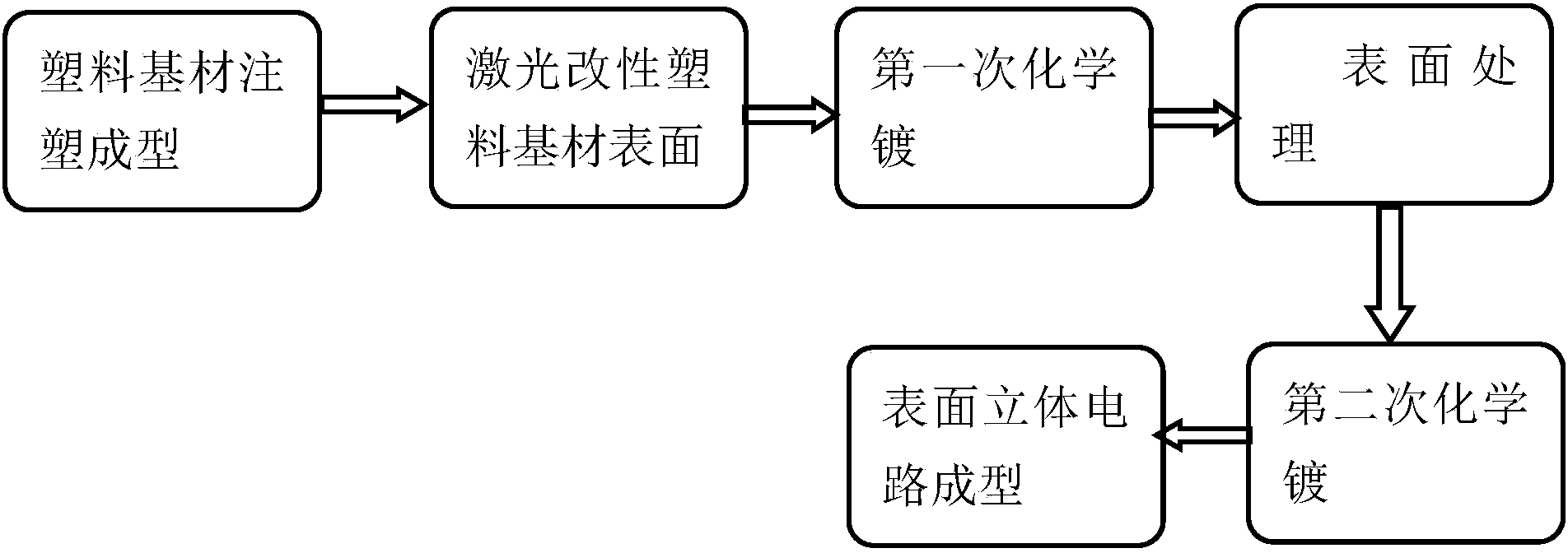
[0033] refer to figure 1 , in some embodiments, the step of three-dimensional circuit manufacturing process comprises:

[0034] Injection molding of plastic base material, laser modification of the surface of plastic base material, first chemical plating, surface treatment, second chemical plating, and surface post-treatment complete the final three-dimensional circuit molding. It should be understood that, in addition to general-purpose plastics, the present invention is also applicable to modified plastics containing modified components.

[0035] Step 1. Injection molding of plastic base material

[0036] Ordinary plastics are injection-molded according to the designed three-dimensional circuit structur...


PUM

PropertyMeasurementUnit
wavelengthaaaaaaaaaa

Abstract

The invention discloses a manufacturing method of a three-dimensional circuit. The method comprises the steps of injection modeling of plastic base materials, laser modification of plastic base material surfaces, first-time chemical plating, surface treatment, second-time chemical plating, surface aftertreatment, and three-dimensional circuit forming. The three-dimensional circuit is obtained through the manufacturing method. By means of the manufacturing method of the three-dimensional circuit, the three-dimensional circuit can be accurately, rapidly and economically formed on a common plastic structural part, and the product cost is greatly reduced.

Description

technical field [0001] The invention relates to the field of circuit production, in particular to a three-dimensional circuit and a production method thereof. Background technique [0002] With the improvement of the integration of electronic equipment, the volume of communication equipment is getting smaller and smaller. It is necessary to reduce the size without significantly affecting the function and efficiency of electronic components. In this context, it is very important to realize the same processing technology as the carrier. important. [0003] The current communication equipment includes call function, wifi function, Bluetooth, GPS, NFC and other functions. All functions that require wireless transmission require the support of antennas. The existing antenna manufacturing processes are as follows: [0004] 1. The antenna is made of FPC and metal sheets. Most of the built-in antennas of mobile phones are composed of metal shrapnel and plastic brackets. This struc...

Claims


Application Information

Patent Timeline
Patent Type & Authority Applications(China)
IPC IPC(8): H05K1/00H05K3/00C23C18/20
Inventor 蔡志祥邹凯杨伟杨玉山
Owner SHENZHEN SUNSHINE LASER & ELECTRONICS TECH CO LTD
Why Eureka
Try Eureka