Crystalline silicon solar cell having doped silicon carbide layer and manufacturing method thereof

A solar cell, silicon carbide layer technology, applied in the field of solar cells, can solve problems such as excessive photon energy loss

Inactive Publication Date: 2015-01-14
NEO SOLAR POWER CORP
View PDF10 Cites 3 Cited by
  • Summary
  • Abstract
  • Description
  • Claims
  • Application Information

AI Technical Summary

Problems solved by technology

However, materials with too small energy gap will have the problem of excessive photon energy loss, so researchers m

Method used


Image

  • Crystalline silicon solar cell having doped silicon carbide layer and manufacturing method thereof
  • Crystalline silicon solar cell having doped silicon carbide layer and manufacturing method thereof
  • Crystalline silicon solar cell having doped silicon carbide layer and manufacturing method thereof

Examples


Embodiment Construction

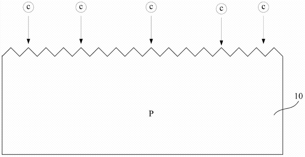
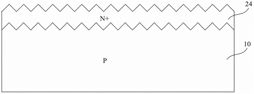
[0027] Please refer to Figure 1A to Figure 1C , which is a schematic diagram of the manufacturing steps of the doped silicon carbide layer of the crystalline silicon solar cell with the doped silicon carbide layer of the present invention. First, a semiconductor substrate 10 with a roughened surface is provided, and carbon elements (carbon elements are represented by C in the figure) are implanted into the first surface of the semiconductor substrate 10 by ion implantation, and then the silicon carbide layer 22 is formed by high temperature annealing. ,Such as Figure 1A , Figure 1B shown. By controlling the amount of energy provided by the carbon element, the depth of the carbon element implanted into the semiconductor substrate is controlled. For example, the implantation depth of the carbon element can be controlled to be less than 2 micrometers (μm), that is, the depth of the silicon carbide layer is 2 μm. Next, the silicon carbide layer 22 is reversely doped with a ...


PUM


Abstract

The present invention discloses a crystalline silicon solar cell having a doped silicon carbide layer and a manufacturing method thereof. The solar cell comprises: a semiconductor substrate having a roughened first surface; a doped silicon carbide layer arranged at the first surface and comprising a doping element; an anti-reflecting layer; a plurality of front electrodes arranged on the anti-reflecting layer and penetrating the anti-reflecting layer; and a back electrode layer arranged at a second surface of the semiconductor substrate. As the doped silicon carbide layer has doping reversed to the doping type of the semiconductor substrate and a silicon carbide element, the doped silicon carbide layer has the characteristics of low resistance and wide energy gap, so that the doped silicon carbide layer can be used as an emitter of the solar cell, in addition, the doped silicon carbide layer has low absorption for sunlight, so that quantity of light entering the semiconductor substrate can be increased, thereby improving photoelectric conversion rate of the solar cell.

Description

technical field [0001] The invention relates to a solar cell, in particular to a crystalline silicon solar cell with a doped silicon carbide layer and a manufacturing method thereof. Background technique [0002] Due to the shortage of petrochemical energy, people's awareness of the importance of environmental protection has increased. Therefore, in recent years, people have been actively researching and developing technologies related to alternative energy and renewable energy, hoping to reduce the current human dependence on petrochemical energy and the impact on the environment when using petrochemical energy. the impact. Among the many alternative energy and renewable energy technologies, solar cells have attracted the most attention. The main reason is that solar cells can directly convert solar energy into electrical energy, and no harmful substances such as carbon dioxide or nitride will be produced during the power generation process, and will not pollute the enviro...

Claims


Application Information

Patent Timeline
IPC IPC(8): H01L31/0224H01L31/18
CPCH01L31/0288H01L31/074H01L31/1804Y02E10/547Y02P70/50
Inventor 戴煜暐陈伟铭洪传献
Owner NEO SOLAR POWER CORP
Why Eureka
Try Eureka