Method for manufacturing vertical type high-power gallium nitride PIN diode
A PIN diode and gallium nitride technology, which is applied in the field of manufacturing vertical high-power gallium nitride PIN diodes, can solve the problems of large chip area, affecting the DC and switching characteristics of components, and not being successfully introduced into the high-power market. The effect of low sensitivity
- Summary
- Abstract
- Description
- Claims
- Application Information
AI Technical Summary
Problems solved by technology
Method used
Image
Examples
Embodiment 1
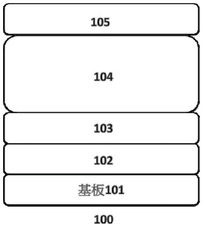
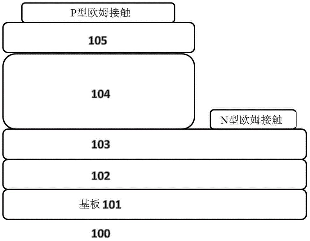
[0035] Such as figure 1 As shown, firstly, a substrate 101 is provided, and the substrate 101 is not particularly limited, and may be commonly used and well-known such as silicon (Si), gallium arsenide (GaAs), sapphire, SiC, and the like. In addition, multiple layers of material layers not shown and serving as various active / passive elements may have been formed on the substrate. Then as figure 1 As shown, a gallium nitride semiconductor stack 102 is formed on the substrate 101 as a buffer layer, and then, the gallium nitride semiconductor stack 102 is grown with a high concentration (1×10 19 cm -3 ) gallium nitride semiconductor layer 103; after that, grow a low concentration (1x10 16 cm -3 ) gallium nitride semiconductor layer 104 (8um), the final high concentration (1x10 18 cm -3 ) GaN semiconductor layer 105 to complete the device structure.
[0036] It can expose the multiple layers of material layers through well-known necessary processes such as photolithography ...
PUM
 Abstract
Description
Claims
Application Information


