Optical attenuator of wave length related loss compensation and compensation method

A wavelength-dependent and loss-compensating technology, applied in the coupling of optical waveguides, light guides, optics, etc., can solve problems such as difficult to low and inability to provide different compensation amounts

Active Publication Date: 2015-01-21
JIANGSU XUHAI OPTO ELECTRONIC TECH CO LTD
View PDF6 Cites 8 Cited by
  • Summary
  • Abstract
  • Description
  • Claims
  • Application Information

AI Technical Summary

Problems solved by technology

[0019] It can be seen that the above wavelength-dependent loss compensation scheme has an inherent disadvantage, that is, it is difficult to obtain generally low wavelength-dependent loss in a large attenuation range (such as 0 to 20dB), which is due to the use of prism-type dispersion elements. Features: such as Figur

Method used


Image

  • Optical attenuator of wave length related loss compensation and compensation method
  • Optical attenuator of wave length related loss compensation and compensation method
  • Optical attenuator of wave length related loss compensation and compensation method

Examples


Embodiment 1

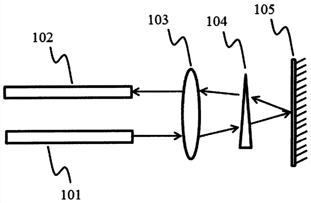
[0068] An embodiment of an optical attenuator for compensating wavelength-dependent loss provided by the present invention, such as Figure 5a (top view) and Figure 5b (Side view), including:

[0069] An input optical waveguide (501) for inputting optical signals;

[0070] An output optical waveguide (502) for outputting optical signals;

[0071] a collimating lens (503) having a first focal plane (522) and a second focal plane (523);

[0072] a mirror (505) having an axis of rotation (521) rotatable about said axis of rotation;

[0073] A phase layer is composed of independent phase plates (504).

[0074] The input optical waveguide and the output optical waveguide are located on the first focal plane of the collimating lens, and the mirror is located on the second focal plane of the collimating lens; the phase plate is located between the first focal plane and the collimating lens, close to input optical waveguide and output optical waveguide,.

[0075] The input opti...

Embodiment 2

[0086] The 2nd embodiment of the present invention is similar to embodiment 1, as Figure 6a and 6b As shown, the difference is that the phase layer (604) is directly formed on the end faces of the input optical waveguide (601) and the output optical waveguide (602) by means of optical coating. The interface (610) between the first optical area (607) and the second optical area (608) can be a straight line or a circle or an annulus.

Embodiment 3

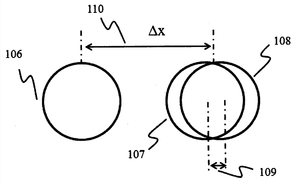
[0088] The 3rd embodiment of the present invention is similar to embodiment 1, as Figure 7 As shown, the difference is that the phase layer (704) is spliced ​​by two optical glasses with different refractive indices. For example, the first optical region (707) adopts optical glass bk7, and the second optical region (708) adopts fused silica. The refractive index difference between the two is about 0.056 in the 1.55 micron wavelength band commonly used in communication. It can be achieved by increasing the thickness (709)t The required optical path difference OPD, OPD is described by the aforementioned formula (10). The interface (710) between the two optical materials needs to be flat enough to avoid unwanted scattering when the light spot passes through. The optical substrate (706) is not necessary in terms of optical effects, it plays a role of supporting the optical materials used in the thinner first and second optical regions, and one of two types of optical glass can b...


PUM


Abstract

The invention relates to a variable optical attenuator for optical communication. A phase layer between a collimating lens and an output optical waveguide layer is introduced, a second wave length related loss approximate to the natural wave length related loss of the optical attenuator and opposite to the natural wave length related loss in signal is generated so as to offset the natural wave length related loss, and the optical attenuator with the extremely low residue wave length related loss is obtained so as to meet the requirement for the optical attenuator of an optical communication system.

Description

technical field [0001] The invention relates to an optical attenuator for optical communication, in particular to a variable optical attenuator for wavelength-dependent loss compensation and a compensation method. Background technique [0002] The variable optical attenuator (hereinafter referred to as the optical attenuator) can quantitatively attenuate the optical signal, and the optical attenuation value can be adjusted according to the needs. It is an important optical device in the modern optical communication system. Microelectromechanical rotating mirror optical attenuators have been widely adopted in modern optical communication networks due to their simple optical design, compact structure, and convenient electrical control. In most applications of optical attenuators, such as wavelength division and dense wavelength division optical networks, optical signals of many wavelengths are transmitted in optical fibers, and optical signals of all these wavelengths need to ...

Claims


Application Information

Patent Timeline
IPC IPC(8): G02B6/32G02B6/26
CPCG02B6/266G02B6/32
Inventor 陈波
Owner JIANGSU XUHAI OPTO ELECTRONIC TECH CO LTD
Why Eureka
Try Eureka