Array substrate, manufacturing method of array substrate and display panel

A technology for array substrates and display panels, applied in semiconductor/solid-state device manufacturing, instruments, semiconductor devices, etc., can solve the problem of reducing the driving voltage of the insulating layer, and achieve the enhancement of horizontal electric field strength, high brightness, and weakening of vertical electric field strength distribution. Effect

Inactive Publication Date: 2015-01-21
BOE TECH GRP CO LTD +1
View PDF6 Cites 10 Cited by
  • Summary
  • Abstract
  • Description
  • Claims
  • Application Information

AI Technical Summary

Problems solved by technology

However, the thickness of the insulating layer 4 decreases every time The driving voltage can only be reduced by 0.5V. For high PPI products, the thickness of the insulating layer 4 itself is already very small, and the range of reducing the driving voltage by reducing the thickness of the insulating layer is very limited

Method used


Image

  • Array substrate, manufacturing method of array substrate and display panel
  • Array substrate, manufacturing method of array substrate and display panel
  • Array substrate, manufacturing method of array substrate and display panel

Examples


Embodiment Construction

[0030] Specific embodiments of the present invention will be described in detail below in conjunction with the accompanying drawings. It should be understood that the specific embodiments described here are only used to illustrate and explain the present invention, and are not intended to limit the present invention.

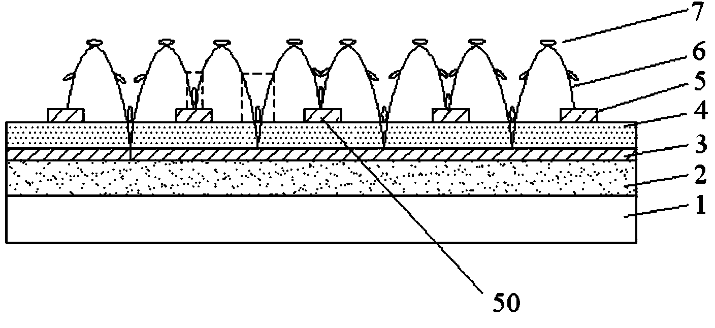
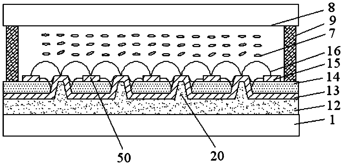
[0031] The present invention firstly provides an array substrate, such as figure 2 As shown in , the array substrate includes a planar layer 12 , a first electrode layer 13 , an insulating layer 14 and a second electrode layer 15 sequentially located above the base substrate 1 (the "base substrate" here includes a thin film transistor array). The second electrode layer 15 includes a plurality of electrode strips 50 , the planar layer 12 includes a plurality of protrusions 20 protruding toward the second electrode layer 15 , and at least a part of the first electrode layer 13 is formed on the protrusions 20 .

[0032] The present invention improves the design o...


PUM


Abstract

The invention discloses an array substrate, a manufacturing method of the array substrate and a display panel and relates to the technical field of display. The array substrate comprises a flat layer, a first electrode layer, an insulating layer and a second electrode layer which are sequentially located above a substrate body. The second electrode layer comprises a plurality of electrode bars, and the flat layer comprises a plurality of protrusions protruding towards the second electrode layer. At least part of the first electrode layer is formed on the protrusions. Preferably, the positions, corresponding to the gaps between the adjacent electrode bars, of the flat layer are designed with protrusions. According to the array substrate, the manufacturing method of the array substrate and the display panel, due to the protrusions designed on the flat layer, the vertical distance between electrodes of the first electrode layer and the second electrode layer is reduced, the effects of improving the horizontal electric field intensity and relieving the perpendicular electric field intensity distribution are achieved, and therefore the display panel can have high brightness under the low driving voltage.

Description

technical field [0001] The present invention relates to the field of display technology, in particular to an array substrate, a manufacturing method thereof, and a display panel including the array substrate. Background technique [0002] In order to satisfy consumers' pursuit of display quality, the resolution of liquid crystal display panels is getting higher and higher, resulting in lower and lower aperture ratios of products and increasing power consumption. [0003] figure 1 It is a structural schematic diagram of an existing array substrate, on which a flat layer 2, a first electrode layer 3, an insulating layer 4 and a second electrode layer 5 are sequentially arranged on a base substrate 1 (the "base substrate" here includes a thin film transistor array) . Wherein, the second electrode layer 5 includes a plurality of electrode strips 50 . [0004] The liquid crystals 7 used in existing high PPI (Pixels Per Inch, number of pixels per inch) products are generally po...

Claims


Application Information

Patent Timeline
Patent Type & Authority Applications(China)
IPC IPC(8): G02F1/1343G02F1/1368H01L27/12H01L21/77
CPCG02F1/134309G02F1/1368H01L27/124H01L27/127G02F1/134363G02F2201/121G02F2201/123G02F1/133345G02F1/13439G02F1/133357G02F1/134345
Inventor 向西姜妮冯远明
Owner BOE TECH GRP CO LTD
Why Eureka
Try Eureka