Array substrate, manufacturing method thereof, and display panel

一种阵列基板、显示面板的技术,应用在半导体/固态器件制造、仪器、半导体器件等方向,能够解决绝缘层降低驱动电压等问题,达到增强水平电场强度、减弱垂直电场强度分布、高亮度的效果

Inactive Publication Date: 2018-05-04
BOE TECH GRP CO LTD +1
View PDF6 Cites 0 Cited by
  • Summary
  • Abstract
  • Description
  • Claims
  • Application Information

AI Technical Summary

Problems solved by technology

However, the thickness of the insulating layer 4 decreases every time The driving voltage can only be reduced by 0.5V. For high PPI products, the thickness of the insulating layer 4 itself is already very small, and the range of reducing the driving voltage by reducing the thickness of the insulating layer is very limited

Method used


Image

  • Array substrate, manufacturing method thereof, and display panel
  • Array substrate, manufacturing method thereof, and display panel
  • Array substrate, manufacturing method thereof, and display panel

Examples


Embodiment Construction

[0030] Specific embodiments of the present invention will be described in detail below in conjunction with the accompanying drawings. It should be understood that the specific embodiments described here are only used to illustrate and explain the present invention, and are not intended to limit the present invention.

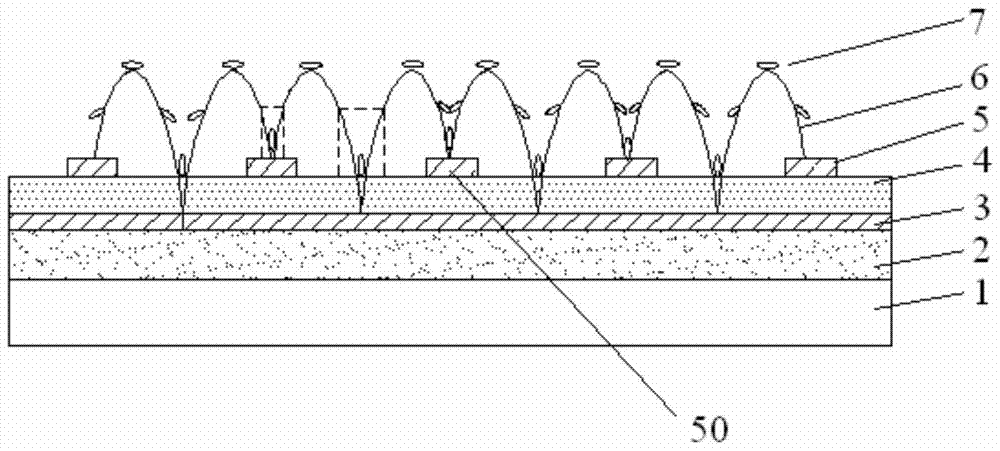
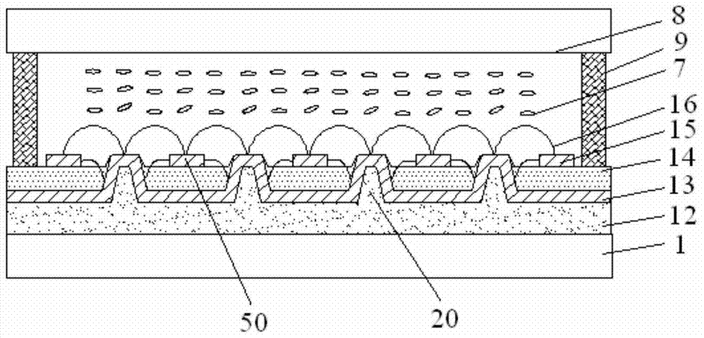
[0031] The present invention firstly provides an array substrate, such as figure 2 As shown in , the array substrate includes a planar layer 12 , a first electrode layer 13 , an insulating layer 14 and a second electrode layer 15 sequentially located above the base substrate 1 (the "base substrate" here includes a thin film transistor array). The second electrode layer 15 includes a plurality of electrode strips 50 , the planar layer 12 includes a plurality of protrusions 20 protruding toward the second electrode layer 15 , and at least a part of the first electrode layer 13 is formed on the protrusions 20 .

[0032] The present invention improves the design o...


PUM

PropertyMeasurementUnit
visible light transmittanceaaaaaaaaaa

Abstract

An array substrate, a fabricating method thereof, and a display panel including the array substrate are provided. The array substrate includes a base substrate (1), a planarization layer (12), and a first electrode layer (13). The planarization layer (12) in on the base substrate (1) and has a plurality of protrusions (20) protruding away from the base substrate (1) and resulting in a plurality of grooves between adjacent protrusions (20). The first electrode layer (13) has at least a portion over the plurality of protrusions (20) of planarization layer (12).

Description

technical field [0001] The present invention relates to the field of display technology, in particular to an array substrate, a manufacturing method thereof, and a display panel including the array substrate. Background technique [0002] In order to satisfy consumers' pursuit of display quality, the resolution of liquid crystal display panels is getting higher and higher, resulting in lower and lower aperture ratios of products and increasing power consumption. [0003] figure 1 It is a structural schematic diagram of an existing array substrate, on which a flat layer 2, a first electrode layer 3, an insulating layer 4 and a second electrode layer 5 are sequentially arranged on a base substrate 1 (the "base substrate" here includes a thin film transistor array) . Wherein, the second electrode layer 5 includes a plurality of electrode strips 50 . [0004] The liquid crystals 7 used in existing high PPI (Pixels Per Inch, number of pixels per inch) products are generally po...

Claims


Application Information

Patent Timeline
Patent Type & Authority Patents(China)
IPC IPC(8): G02F1/1343G02F1/1368H01L27/12H01L21/77
CPCG02F1/134309G02F1/1368H01L27/124H01L27/127G02F1/134363G02F2201/121G02F2201/123G02F1/133345G02F1/13439G02F1/133357G02F1/134345
Inventor 向西姜妮冯远明
Owner BOE TECH GRP CO LTD
Why Eureka
Try Eureka