Wavefront control chip based on electronic control liquid crystal plane micro lens

A technology for controlling chips and microlenses, applied in instruments, optics, static indicators, etc., can solve problems such as lack of fine control, and achieve the effects of flexible adjustment methods, high control accuracy, and easy matching and coupling

Active Publication Date: 2015-01-21
HUAZHONG UNIV OF SCI & TECH
View PDF6 Cites 14 Cited by
  • Summary
  • Abstract
  • Description
  • Claims
  • Application Information

AI Technical Summary

Problems solved by technology

However, there is still a lack of the ability to finely adjust and transform the wavefront and to construct complex wavefronts based on small miniaturization means

Method used


Image

  • Wavefront control chip based on electronic control liquid crystal plane micro lens
  • Wavefront control chip based on electronic control liquid crystal plane micro lens
  • Wavefront control chip based on electronic control liquid crystal plane micro lens

Examples


Embodiment Construction

[0028] In order to make the object, technical solution and advantages of the present invention clearer, the present invention will be further described in detail below in conjunction with the accompanying drawings and embodiments. It should be understood that the specific embodiments described here are only used to explain the present invention, not to limit the present invention. In addition, the technical features involved in the various embodiments of the present invention described below can be combined with each other as long as they do not constitute a conflict with each other.

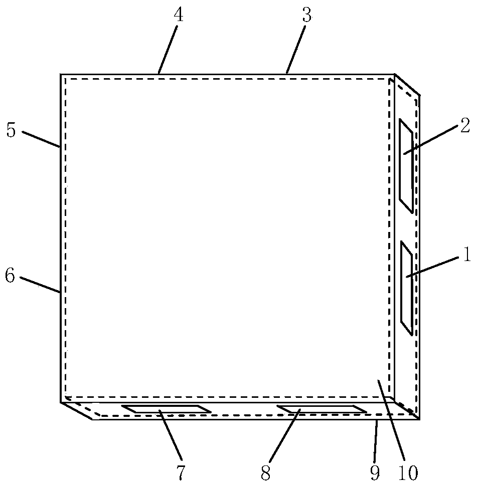
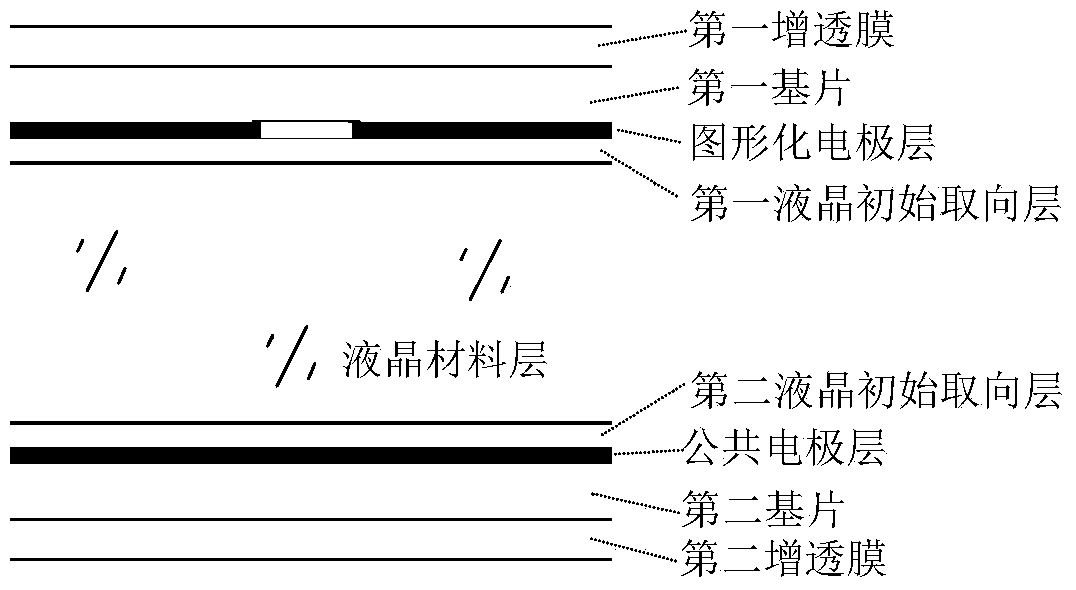
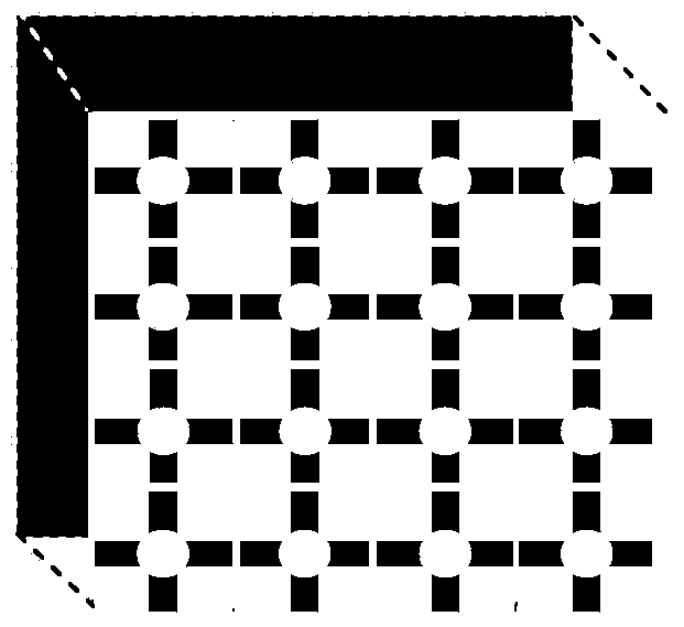
[0029] Such as figure 1 As shown, the wavefront control chip based on the electronically controlled liquid crystal planar microlens according to the embodiment of the present invention includes a chip housing 9 and an area array electrically controlled liquid crystal planar microlens 10 . The area array electronically controlled liquid crystal planar microlens 10 is packaged in the chip casing ...


PUM

PropertyMeasurementUnit
porosityaaaaaaaaaa

Abstract

The invention discloses a wavefront control chip based on an electronic control liquid crystal plane micro lens. The chip comprises the area relay electronic control liquid crystal plane micro lens. The area relay electronic control liquid crystal plane micro lens comprises a liquid crystal material layer, a first liquid crystal initial orientation layer, a graphical electrode layer, a first substrate, a first antireflection film, a second liquid crystal initial orientation layer, a public electrode layer, a second substrate and a second antireflection film, the first liquid crystal initial orientation layer, the graphical electrode layer, the first substrate and the first antireflection film are sequentially arranged on the upper surface of the liquid crystal material layer, and the second liquid crystal initial orientation layer, the public electrode layer, the second substrate and the second antireflection film are sequentially arranged on the lower surface of the liquid crystal material layer. The public electrode layer is composed of a homogeneous conducting film. The graphical electrode layer is composed of sub-electrodes distributed in an m*n-ary array, each sub-electrode is composed of four strip-shaped conducting films evenly distributed around the circumference in a cross shape, and the strip-shaped conducting films in each sub-electrode are not in contact. Wavefront controlled modulation or solidification or checking or search or tracking and complex wavefront construction can be achieved, and the chip can be coupled with other optical and photoelectric structures and electronic and mechanical devices easily, and is good in environmental suitability.

Description

technical field [0001] The invention belongs to the technical field of optical precision measurement and control, and more specifically relates to a wavefront control chip based on an area array electronically controlled liquid crystal plane microlens for electronically controlling and adjusting an incident wavefront. Background technique [0002] The wave front is a basic physical parameter that characterizes light waves, and is one of the key physical elements that control the shape and evolution of light beams. The basic ones, such as converging spherical or cylindrical wavefronts, diverging spherical or cylindrical wavefronts, or plane wavefronts, will guide and constrain light waves into spherical or cylindrical beamforming, spherical or cylindrical diverging forms, or parallel beams. Generally speaking, any complex light wave can be represented by sub-wavefront fitting based on the localized segmentation of the above-mentioned spherical, cylindrical or planar wavefront...

Claims


Application Information

Patent Timeline
Patent Type & Authority Applications(China)
IPC IPC(8): G02F1/1343G02F1/133G02F1/29G01J3/12
CPCG02F1/13306G02F1/134309G02F1/29
Inventor 张新宇佟庆雷宇罗俊桑红石谢长生
Owner HUAZHONG UNIV OF SCI & TECH
Why Eureka
Try Eureka