Chip testing equipment with high universality

A chip testing and universal technology, applied in the direction of single semiconductor device testing, measuring device casing, etc., can solve the problems of difficult chip electrical performance testing, poor applicability, and lack of high versatility, so as to achieve fast chip testing and improve product universality sexual effect

Inactive Publication Date: 2015-01-28
SHANDONG SINOCHIP SEMICON
View PDF5 Cites 15 Cited by
  • Summary
  • Abstract
  • Description
  • Claims
  • Application Information

AI Technical Summary

Problems solved by technology

However, in this structure, on the one hand, a large amount of capital investment is required to modify the separate test equipment to make it suitable for chips of a specific size, a specific number of external pins, and a specific package type, that is, for tests of different sizes, the versatility is poor; on the other hand , It takes a long time to modify the test equipment for different chips, and it takes a long time to put it on the market. It is not suitable for large investme

Method used


Image

  • Chip testing equipment with high universality
  • Chip testing equipment with high universality
  • Chip testing equipment with high universality

Examples


Embodiment Construction

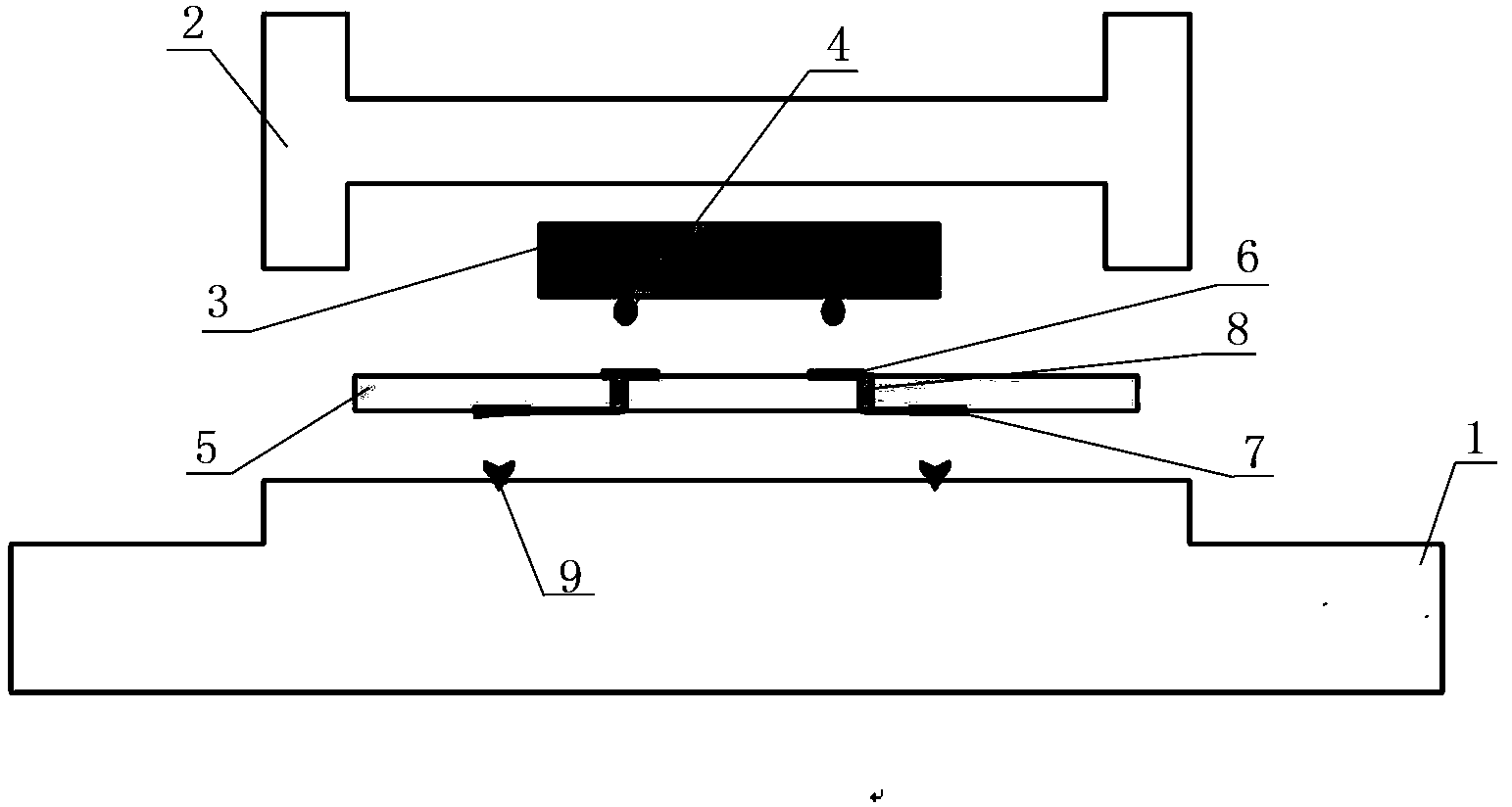
[0018] The present invention will be further described below in conjunction with the accompanying drawings and embodiments.

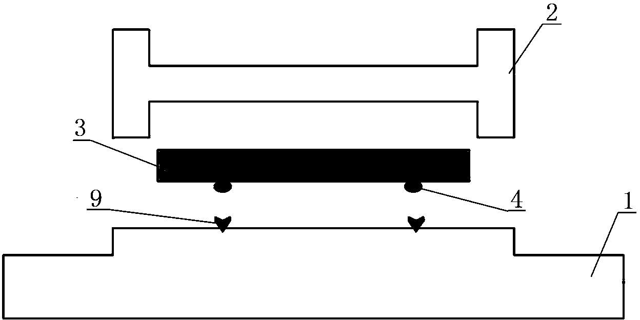
[0019] Such as figure 1 As shown, the structure diagram of the existing chip electrical performance testing equipment is given, which is composed of a chip connector 1 and a chip presser 2. The chip connector 1 is provided with a test connection point 9, and the test connection point 9 is connected to the chip tester. The device is connected. The distribution position of the test connection point 9 on the chip connector 1 is consistent with the distribution of the external pins 4 on the chip 3 to be tested, and the chip presser 2 is pressed on the top of the chip 3 to be tested to ensure that the external pins 4 Stable electrical connection with test connection point 9 to realize chip testing.

[0020] for figure 1 For the test equipment given in , for different types of chips, due to their different package types, package sizes, and pin numbers, whe...


PUM


Abstract

The invention provides chip testing equipment with high universality. The chip testing equipment with high universality comprises a chip connector, a chip press-fit device and a chip testing equipment body, and is characterized by further comprising a testing adapter plate. Lower surface contact points matched with testing connecting points are arranged on one surface of the testing adapter plate, upper surface contact points which are consistent with external pins of a chip to be tested in distribution are arranged on the other surface of the testing adapter plate, and the lower surface contact points are connected with the upper surface contact points. The chip electric performance testing equipment can effectively test the chip, when coordinates and the number of the external pins of the chip to be tested change due to the changes of the encapsulated type and the encapsulated size of the chip and the number of the pins, just the corresponding testing adapter plate needs to be replaced, and therefore the product universality of a testing machine is improved, a great amount of time and capital investment needed by modification of the testing machine for each kind of product are avoided, and chips can be tested rapidly.

Description

technical field [0001] The present invention relates to a chip testing device with high versatility, and more specifically, to a chip testing device with high versatility, which realizes the transfer of external pins of the chip through a test adapter board. Background technique [0002] With the vigorous development of the semiconductor industry, there are large differences in chip types, pin numbers, distribution, package types, and package sizes. After the chip is packaged, electrical performance testing is required to screen chips with good functions. [0003] Generally speaking, in the known chip test technology, the structure of common test equipment is as follows figure 1 As shown, in view of different chip package types, different package sizes, different numbers of external pins, and differences in the coordinates of the external pins, it is necessary to specially design and process the matching test component chip connector 1 to realize the electrical performance ...

Claims


Application Information

Patent Timeline
IPC IPC(8): G01R31/26G01R1/04
Inventor 乔帅栗振超刘昭麟王璐孟新玲
Owner SHANDONG SINOCHIP SEMICON
Why Eureka
Try Eureka