3D display structure and manufacturing method thereof
A technology of display structure and manufacturing method, applied in optical components, optics, instruments, etc., can solve problems such as low bonding yield, high manufacturing cost, and damage to the 3D optical structure of 3D screens
- Summary
- Abstract
- Description
- Claims
- Application Information
AI Technical Summary
Problems solved by technology
Method used
Image

Examples
Embodiment 1
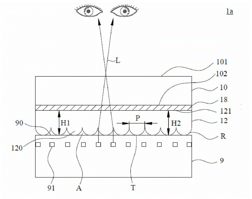
[0044] figure 1 It is a schematic diagram of a 3D display structure according to an embodiment of the present invention. See figure 1 . A 3D display structure 1a is suitable for a display module 9 having a display surface 90, and includes a light-transmitting layer 10 and a 3D display layer 12. For the convenience of description, the display module 9 of this embodiment is illustrated by a liquid crystal display module (LCD Module, LCM), and the 3D display structure 1a is realized by, for example, a 3D display panel or a 3D display film. In other embodiments, the display module 9 is, for example, an LCD panel, a touch display of a digital TV, a display or touch display of a notebook computer, a display or touch display of an ATM cash machine, or a display of other household equipment or For the touch display, this embodiment does not limit the aspect of the 3D display structure 1a and the display module 9.
[0045] In practice, the high-hardness transparent layer 10 is connected...
Embodiment 2
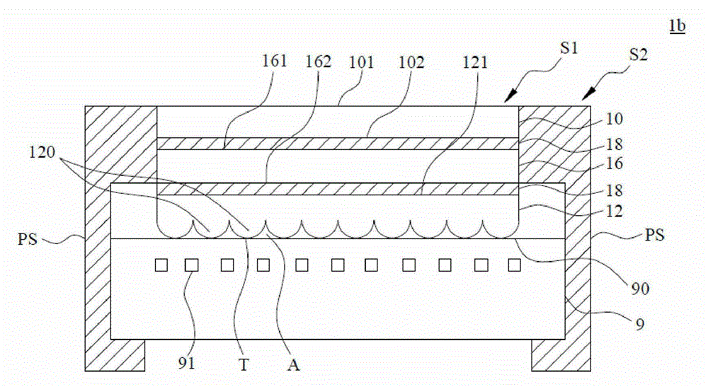
[0064] figure 2 It is a schematic diagram of a 3D display structure according to another embodiment of the present invention. See figure 2 . among them figure 2 versus figure 1 The 3D display structures 1b and 1a are similar in structure. For example, the display module 9 outputs a 3D image through the 3D display structure 1b, and the viewer can see or enjoy the 3D image naked. The difference between the 3D display structures 1b and 1a is that the 3D display structure 1b further includes an atomization layer 16. The light-transmitting layer 10 covers the fogging layer 16, and the fogging layer 16 covers the 3D display layer 12. In other words, the fogging layer 16 is connected between the transparent layer 10 and the 3D display layer 12.
[0065] In detail, a 3D display structure 1b is suitable for a display module 9 with a display surface 90 and includes: a light-transmitting layer 10, an fogging layer 16 and a 3D display layer 12. In practice, the light-transmitting layer...
Embodiment 3
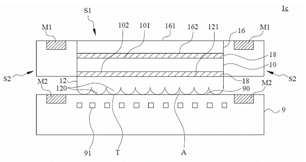
[0071] image 3 It is a schematic diagram of a 3D display structure according to another embodiment of the present invention. See image 3 . among them image 3 versus figure 1 The 3D display structures in 1c and 1a are similar in structure. The difference between the 3D display structures 1c and 1a is that the fogging layer 16 is connected to and covers the transparent layer 10. The 3D display structure 1c is fixed to the display module 9 through a plurality of magnetic attraction elements M1.
[0072] In detail, a 3D display structure 1c is suitable for a display module 9 having a display surface 90, and includes: a light-transmitting layer 10, an fogging layer 16 and a 3D display layer 12. In practice, the light-transmitting layer 10 has a first surface 101 and a second surface 102 opposite to the first surface 101. The atomization layer 16 has a first atomization surface 161 and a second atomization surface 162.
[0073] The 3D display layer 12 has a first bonding surface 1...
PUM
| Property | Measurement | Unit |
|---|---|---|
| Thickness | aaaaa | aaaaa |
| Flatness | aaaaa | aaaaa |
| Moh's hardness | aaaaa | aaaaa |
Abstract
Description
Claims
Application Information
 - R&D
- Intellectual Property
- Life Sciences
- Materials
- Tech Scout
- Unparalleled Data Quality
- Higher Quality Content
- 60% Fewer Hallucinations
Browse by: Latest US Patents, China's latest patents, Technical Efficacy Thesaurus, Application Domain, Technology Topic, Popular Technical Reports.
© 2025 PatSnap. All rights reserved.Legal|Privacy policy|Modern Slavery Act Transparency Statement|Sitemap|About US| Contact US: help@patsnap.com