Unlock instant, AI-driven research and patent intelligence for your innovation.

Mother board, mother board after box pairing, corresponding manufacturing method and liquid crystal display panel

A motherboard and substrate substrate technology, applied in the direction of instruments, nonlinear optics, optics, etc., can solve problems such as low transmittance, inability to check to confirm alignment accuracy, difficult to cut accurately, etc.

Active Publication Date: 2015-02-04
BOE TECH GRP CO LTD +1
View PDF6 Cites 29 Cited by
  • Summary
  • Abstract
  • Description
  • Claims
  • Application Information

AI Technical Summary

Problems solved by technology

However, during the actual operation of the above method, the cut-type sealant applied along the cut line will cover the alignment mark located near the cut line. Since the cut-type sealant is not transparent, the alignment mark cannot be recognized, so , it is difficult to accurately cut the mother board after the box is cut into the liquid crystal display panel, and when the liquid crystal display panel has defects such as color mixing and low transmittance, it is impossible to check through the alignment mark to confirm whether the above defects are It is caused by poor alignment accuracy

Method used


Image

  • Mother board, mother board after box pairing, corresponding manufacturing method and liquid crystal display panel
  • Mother board, mother board after box pairing, corresponding manufacturing method and liquid crystal display panel
  • Mother board, mother board after box pairing, corresponding manufacturing method and liquid crystal display panel

Examples


Embodiment Construction

[0044] The specific implementations of the motherboard provided by the embodiments of the present invention, the motherboard after the box, the corresponding manufacturing method, and the liquid crystal display panel will be described in detail below in conjunction with the accompanying drawings.

[0045] The shape and thickness of each film layer in the drawings do not reflect the true ratio of the array substrate or the counter substrate, and are only intended to illustrate the content of the present invention.

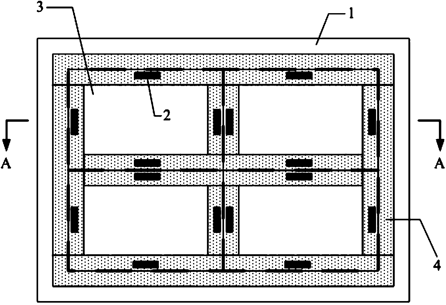
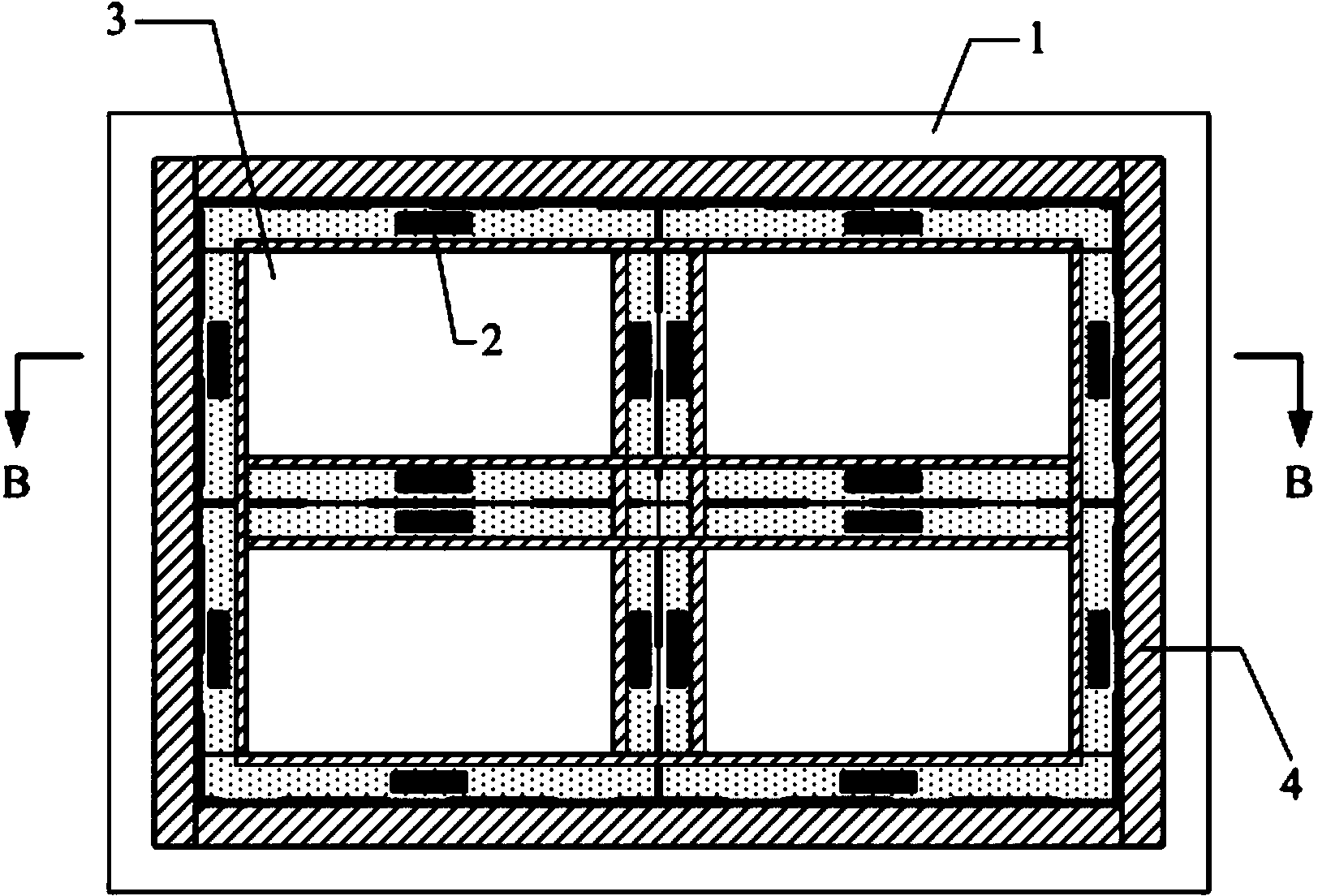
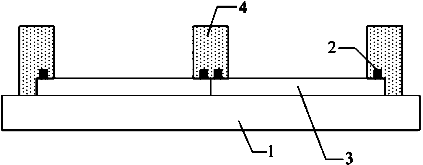
[0046] A motherboard provided by an embodiment of the present invention, such as Figure 1a , Figure 1b , Figure 2a with Figure 2b Shown, where, Figure 2a for Figure 1a A cross-sectional view along the AA direction, Figure 2b for Figure 1b A cross-sectional view along the BB direction, including: a base substrate 1 and a plurality of substrate units 3 with alignment marks 2 arranged in a matrix on the base substrate 1 ( Figure 1a with Figure 1b Take the substrate uni...


PUM


Abstract

The invention discloses a mother board, a mother board after box pairing, a corresponding manufacturing method and a liquid crystal display panel. The mother board comprises a lining baseboard and a plurality of baseboard units which are located on the lining baseboard in a matrix mode and provided with counterpoint marks, wherein frame sealing glue is coated along the cutting line of the lining baseboard, the counterpoint marks are located inside the area of the frame sealing glue, due to the fact that at least the frame sealing glue coated at the counterpoint mark position is transparent frame sealing glue, or the frame sealing glue coated at the counterpoint mark position is the transparent frame sealing glue, the frame sealing glue coated at the area except the counterpoint marks is the transparent or non-transparent frame sealing glue, so that even the frame sealing glue is coated along the cutting line, the counterpoint marks are covered by the frame sealing glue, the problem that the counterpoint marks cannot be identified does not occur, the mother board after box pairing can be accurately cut, and the mother board can be detected and identified through the counterpoint marks when the bad phenomena of color mixing and lower transmitting rate occur on the liquid crystal display panel.

Description

Technical field [0001] The present invention relates to the field of display technology, and in particular to a motherboard, a motherboard after box alignment, a corresponding manufacturing method and a liquid crystal display panel. Background technique [0002] The liquid crystal display panel is mainly composed of a counter substrate, an array substrate, and a liquid crystal layer located between the two substrates. In the actual manufacturing process of the liquid crystal display panel, first, a plurality of opposed substrate units and a plurality of array substrate units arranged in a matrix are respectively fabricated on two motherboards, and then, one of the motherboards is coated and sealed. For frame glue, liquid crystal molecules are dripped on another motherboard, and the box matching process is performed. Finally, the two motherboards are cut along the cutting lines of the two motherboards to form a plurality of liquid crystal display panels. [0003] At present, in ord...

Claims


Application Information

Patent Timeline
IPC IPC(8): G02F1/1333G02F1/1339
CPCG02F1/1333G02F1/1339G02F1/13398
Inventor 姜妮向西李坤
Owner BOE TECH GRP CO LTD
Features
  • R&D
  • Intellectual Property
  • Life Sciences
  • Materials
  • Tech Scout
  • Unparalleled Data Quality
  • Higher Quality Content
  • 60% Fewer Hallucinations
Learn More