Methods of Tungsten Deposition

A kind of chemical vapor deposition, deposition technology

Active Publication Date: 2017-06-06
SHANGHAI HUAHONG GRACE SEMICON MFG CORP
View PDF6 Cites 0 Cited by
  • Summary
  • Abstract
  • Description
  • Claims
  • Application Information

AI Technical Summary

Problems solved by technology

However, the process of this method is too complicated, the time taken by the machine is too long, and the cost is too expensive

Method used


Image

  • Methods of Tungsten Deposition
  • Methods of Tungsten Deposition
  • Methods of Tungsten Deposition

Examples


Embodiment Construction

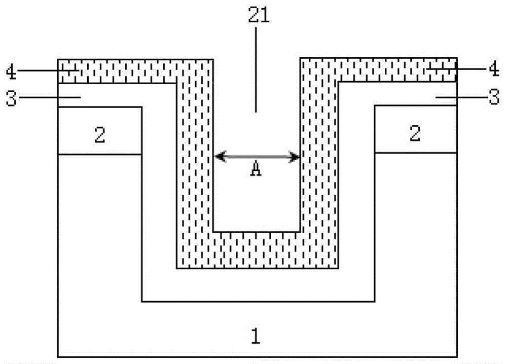
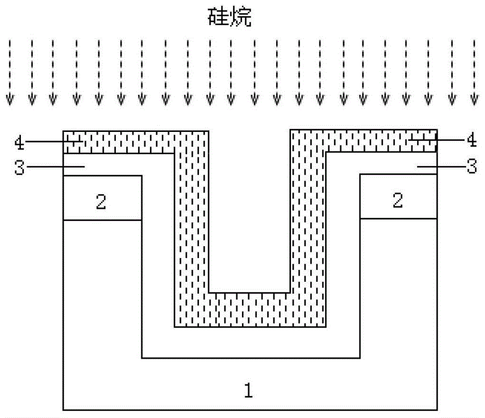
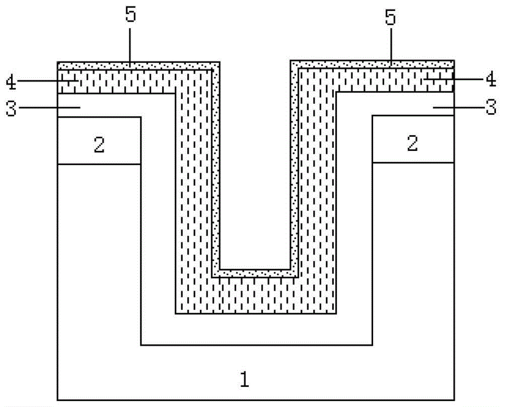
[0043] The method for tungsten deposition of the present invention comprises the steps of:

[0044] (1) On the silicon wafer 1, a layer of dielectric film 2 is deposited by subatmospheric pressure chemical vapor deposition, plasma enhanced chemical vapor deposition, high density plasma chemical vapor deposition or similar methods;

[0045] Wherein, the material of the dielectric film 2 includes: silicon dioxide, doped silicon dioxide or a combined material composed of silicon dioxide and doped silicon dioxide. The doping elements include: phosphorus, boron, fluorine, carbon or combinations thereof.

[0046] Composite materials consisting of silicon dioxide and doped silicon dioxide can be prepared by depositing doped silicon dioxide on undoped silicon dioxide, or by depositing undoped silicon dioxide on doped silicon dioxide. Doped silica, or their composite materials formed by repeated cycle deposition combinations.

[0047] (2) The pattern 21 of the dielectric film 2 is defi...


PUM

PropertyMeasurementUnit
thicknessaaaaaaaaaa
thicknessaaaaaaaaaa
thicknessaaaaaaaaaa

Abstract

The invention discloses a tungsten deposition method, which comprises the following steps that (1) a layer of dielectric film is deposited on a silicon chip; (2) a photoetching process is used for carrying out pattern definition on the dielectric film, in addition, a layer of metal adhesion layer is deposited on the surface of the dielectric film with the defined pattern and the bottom and the side wall of the defined pattern, and then, a layer of metal blocking layer is deposited on the surface of the metal adhesion layer; (3) the silicon chip is transmitted into a reaction cavity A, metal tungsten is deposited on the surface of the metal blocking layer, and in addition, the metal tungsten reaches the specified thickness; (4) the silicon chip is transmitted to an etching cavity B to be treated by an etching process; (5) then, the silicon chip is transmitted into the reaction cavity A for further metal tungsten deposition. The tungsten deposition method has the advantages that a series of technical problems brought by excessive metal tungsten deposition thickness can be avoided, the flow process is simplified, the cost is reduced, and meanwhile, the performance of a device is ensured.

Description

technical field [0001] The invention relates to a metal deposition method in a semiconductor integrated circuit, in particular to a tungsten deposition method. Background technique [0002] In the manufacture of semiconductor integrated circuits, multi-layer metallization technology has produced billions of metal vias. These electrical vias usually use metal as a connection to form an electrical path between two layers of metal; on the other hand, contact The technology of electrical vias is also widely used in the connection between silicon devices and the first layer of metal. Metal tungsten is the best material for through-hole connection due to its good thermal stability, anti-electromigration and simplicity of deposition process. [0003] The conventional tungsten growth technique is a chemical vapor deposition technique. In semiconductor industry manufacturing, the growth substrate of tungsten metal is generally the so-called metal barrier layer (barrier layer), usua...

Claims


Application Information

Patent Timeline
Patent Type & Authority Patents(China)
IPC IPC(8): H01L21/768
CPCH01L21/76877H01L2221/1068
Inventor 成鑫华
Owner SHANGHAI HUAHONG GRACE SEMICON MFG CORP
Why Eureka
Try Eureka