TFT (thin film transistor) substrate and manufacturing method thereof

A manufacturing method and substrate technology, applied in nonlinear optics, instruments, optics, etc., can solve the problems of light leakage, affecting the shading effect of the black matrix 101, reducing the contrast of the panel, etc., to achieve the effect of ensuring the shading effect

Active Publication Date: 2015-02-18
SHENZHEN CHINA STAR OPTOELECTRONICS TECH CO LTD
View PDF5 Cites 8 Cited by
  • Summary
  • Abstract
  • Description
  • Claims
  • Application Information

AI Technical Summary

Problems solved by technology

[0003] In curved TV applications, due to the bending of the panel to a certain extent, there will be a relative misalignment between the TFT (Thin Film Transistor, Thin Film Transistor) substrate and the CF (color filter) substrate that make up the panel, resulting in The light shielding effect of the black matrix (Black Matrix, BM) on the CF substrate is affected
For details, please refer to figure 1 and figure 2 As shown, among them, figure 1 is the shading situation of the black matrix 101 when the panel 100 is not bent, figure 2 After the panel 100 is bent, the shading situation of the black matrix 101 is given by figure 1 and figure 2 It can be seen that after the panel 100 is bent, part of the light is emitted from the side of the black matrix 101, resulting in light leakage, affecting the light shielding effect of the black matrix 101, thereby reducing the contrast of the panel

Method used


Image

  • TFT (thin film transistor) substrate and manufacturing method thereof
  • TFT (thin film transistor) substrate and manufacturing method thereof
  • TFT (thin film transistor) substrate and manufacturing method thereof

Examples


Embodiment Construction

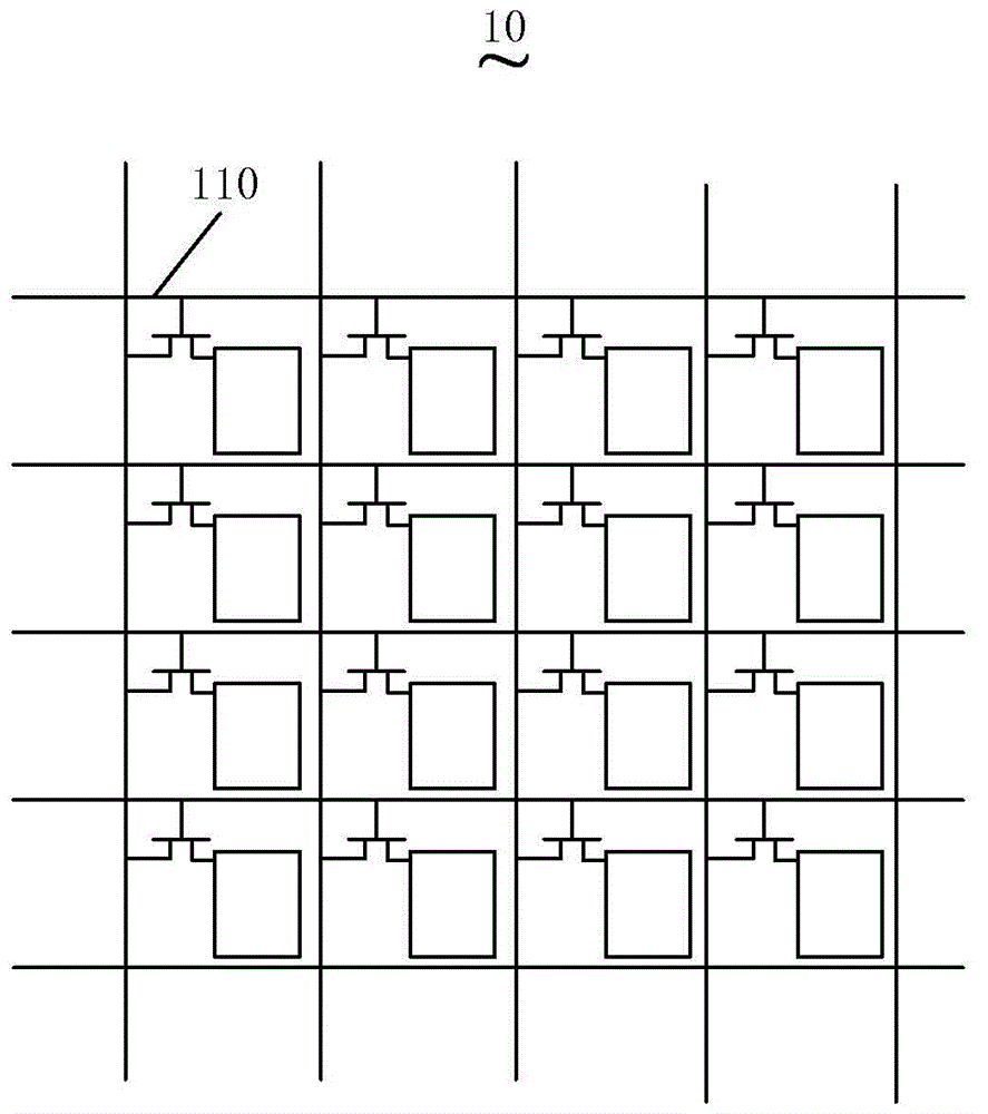
[0028] see image 3 , image 3 It is a schematic structural diagram of a TFT substrate provided by an embodiment of the present invention. The TFT substrate 10 of the embodiment of the present invention includes a plurality of pixel units 110, wherein each pixel unit 110 has the same structure. The structure of one of the pixel units 110 will be described below as an example.

[0029] Please also refer to Figure 4-Figure 7 , Figure 4 yes image 3 A schematic structural diagram of one of the pixel units of the TFT substrate shown, Figure 5 yes Figure 4 The cross-sectional view of the pixel unit shown along the dotted line EF, Figure 6 yes Figure 5 A magnified view of the region A shown, Figure 7 yes Figure 5 A magnified view of region B is shown. first as Figure 4 and Figure 5 As shown, the pixel unit 110 of the embodiment of the present invention includes a substrate 11, a gate electrode 12, a first insulating layer 13, an active layer 14, a black matrix ...


PUM


Abstract

The invention discloses a TFT (thin film transistor) substrate and a manufacturing method thereof. The method comprises the following steps of providing a substrate; forming a gate electrode on the substrate; forming a first insulating layer and an active layer in sequence on the gate electrode; forming a first black matrix on the active layer; forming a source electrode and a drain electrode on the first black matrix; forming second insulating layers on the source electrode and the drain electrode; forming pixel electrodes on the second insulating layers, wherein the pixel electrodes are electrically connected with one of the source electrode and the drain electrode through the corresponding second insulating layer. By the mode, the shading effect of a display panel formed by the TFT substrate can be guaranteed; furthermore, coupling capacitance between data lines and scanning lines is reduced.

Description

technical field [0001] The invention relates to the field of display technology, in particular to a TFT substrate and a manufacturing method thereof. Background technique [0002] Curved TVs are becoming more and more popular due to their better contrast ratio, wider viewing angles and immersive experience, which provide users with a deeper viewing experience. [0003] In curved TV applications, due to the bending of the panel to a certain extent, there will be a relative misalignment between the TFT (Thin Film Transistor, Thin Film Transistor) substrate and the CF (color filter) substrate that make up the panel, resulting in The light shielding effect of the black matrix (Black Matrix, BM) on the CF substrate is affected. For details, please refer to figure 1 and figure 2 As shown, among them, figure 1 is the shading situation of the black matrix 101 when the panel 100 is not bent, figure 2 After the panel 100 is bent, the shading situation of the black matrix 101 is...

Claims


Application Information

Patent Timeline
Patent Type & Authority Applications(China)
IPC IPC(8): G02F1/1335G02F1/1368G02F1/1333
CPCG02F1/1333G02F1/1335G02F1/1368G02F1/136209G02F1/134309G02F1/136227G02F1/136286G02F2201/123
Inventor 连水池熊源
Owner SHENZHEN CHINA STAR OPTOELECTRONICS TECH CO LTD
Why Eureka
Try Eureka