Packaging structure and manufacturing method thereof and display panel

A packaging structure and display panel technology, applied in semiconductor/solid-state device manufacturing, semiconductor devices, electrical components, etc., can solve problems affecting the sealing performance of the packaging structure, production yield, and structural damage of the sintered part 230, etc., to reduce high temperature and stress , Guarantee airtightness, improve the effect of production yield

Inactive Publication Date: 2015-02-18
EVERDISPLAY OPTRONICS (SHANGHAI) CO LTD
View PDF8 Cites 8 Cited by
  • Summary
  • Abstract
  • Description
  • Claims
  • Application Information

AI Technical Summary

Problems solved by technology

However, when the sintered part 230 is laser sintered, the laser treatment is performed on the outer surface of the cover plate 120 corresponding to the width of the sintered part 230. Since the laser irradiates the entire surface of the sintered part 230, high temperature will be generated and cause The structure under the sintering part 230 is damaged, which seriously affects the sealing performance of the package structure and the production yield of the subsequent process

Method used


Image

  • Packaging structure and manufacturing method thereof and display panel
  • Packaging structure and manufacturing method thereof and display panel
  • Packaging structure and manufacturing method thereof and display panel

Examples


Embodiment Construction

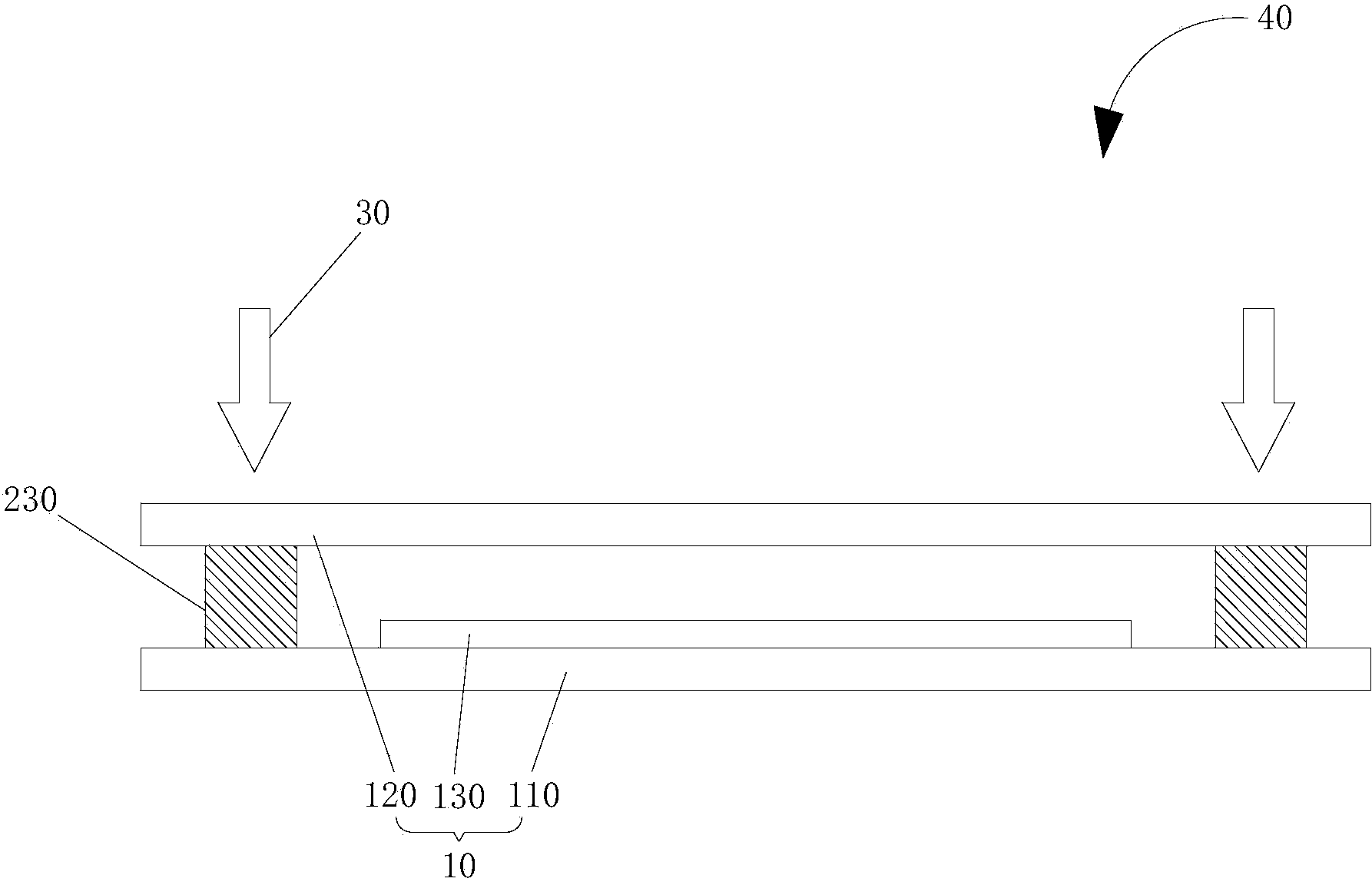
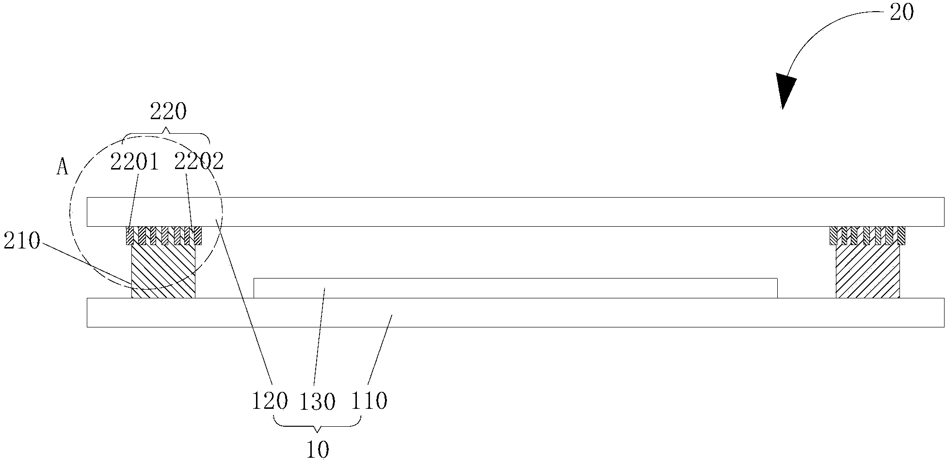
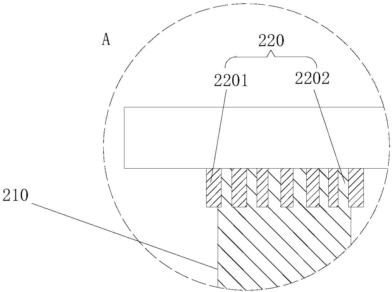
[0060] Such as Figure 2A and 2B As shown, the packaging structure 20 of the present invention is used to seal a display panel 10. The display panel 10 includes a substrate 110, a cover plate 120, and a light-emitting display unit 130 disposed on the surface of the substrate 110. The packaging structure 20 It includes: a sintering part 210, the sintering part 210 is formed between the substrate 110 and the cover plate 120; a protection part 220 is formed between the cover plate 120 and the sintering part 210 and the The sintering part 210 is partially covered, so that the part of the sintering part 210 not covered by the protection part 220 is bonded to the cover plate 120, so as to seal the light-emitting display unit 130 on the substrate 110, the cover plate 120, In a space surrounded by the sintering part 210 and the protection part 220 .

[0061] In the packaging structure 20 of the present invention, a protective portion 220 is additionally provided between the sintered...


PUM


Abstract

The invention discloses a packaging structure and a manufacturing method thereof and a display panel. The packaging structure comprises a sintered proportion and a protective portion; the sintered portion is provided between a substrate and a cover plate; the protective portion is provided between the cover plate and the sintered portion and covers part of the sintered portion so that the part, uncovered by the protective portion, of the sintered portion is connected with the cover plate and that a light-emitting display unit is sealed in space formed by the substrate, the cover plate, the sintered portion and the protective portion. The protective portion provided between the sintered portion and the cover plate covers the upper portion of the sintered portion and divides the sintered portion into a non-sintered area and a sintered area, sintering area of the sintered portion under laser radiation is controlled, high temperature and stress occurring in the laser sintering process are reduced, the structure under the sintered portion is protected from damage caused by high temperature, tightness of the packaging structure is guaranteed, and yield is increased.

Description

technical field [0001] The present invention relates to a packaging structure, a manufacturing method thereof, and a display panel, and in particular to a packaging structure for organic light-emitting display (OLED) technology, a manufacturing method thereof, and a display panel. Background technique [0002] With the development of science and technology, organic materials are widely used in various circuit components. For example, an organic light-emitting display (OLED) made of organic materials has a simple structure and excellent operating temperature, contrast, viewing angle and It has the advantages of light-emitting diode (LED) rectification and light-emitting characteristics, and gradually attracts attention in the display market. Since organic light-emitting displays use light-emitting components made of organic materials to generate light sources, they are highly sensitive to moisture. Once moisture comes into contact with organic light-emitting components, it wi...

Claims


Application Information

Patent Timeline
Patent Type & Authority Applications(China)
IPC IPC(8): H01L51/52H01L51/56H01L27/32
CPCH10K50/841H10K50/8426H10K71/00H10K50/844
Inventor 林茂仲谢博钧张良睿孙新然
Owner EVERDISPLAY OPTRONICS (SHANGHAI) CO LTD
Why Eureka
Try Eureka