A method of manufacturing a light-emitting diode with light emitting electrodes

A technology for light-emitting diodes and a manufacturing method, which is applied to circuits, electrical components, semiconductor devices, etc., can solve the problems of increasing the luminous capacity of the active layer and the large light-blocking area, and achieves improving external quantum efficiency, reducing light-blocking area, and increasing extraction. rate effect

Active Publication Date: 2017-03-29
XIAMEN CHANGELIGHT CO LTD
View PDF7 Cites 0 Cited by
  • Summary
  • Abstract
  • Description
  • Claims
  • Application Information

AI Technical Summary

Problems solved by technology

[0004] However, LEDs are basically provided with soldering station electrodes on the top, and there is a large light-shielding area
In traditional technology, in order to reduce the influence of the shading of the electrode of the soldering station, the most common method is to set a current blocking area under the electrode to block the transmission capacity of the current directly under the electrode of the soldering station, so as to increase the current density in the non-soldering station electrode area. Increase the luminous ability of the active layer and reduce the problem of light blocking of the electrode of the soldering station
However, this method still cannot avoid the light blocking of the soldering station electrodes, and as the brightness of the light-emitting diodes continues to increase, the problem of light blocking of the soldering station electrodes becomes more obvious

Method used


Image

  • A method of manufacturing a light-emitting diode with light emitting electrodes
  • A method of manufacturing a light-emitting diode with light emitting electrodes
  • A method of manufacturing a light-emitting diode with light emitting electrodes

Examples


Embodiment 1

[0084] The invention discloses a method for manufacturing a light-emitting diode with electrode light output, and the specific steps are as follows:

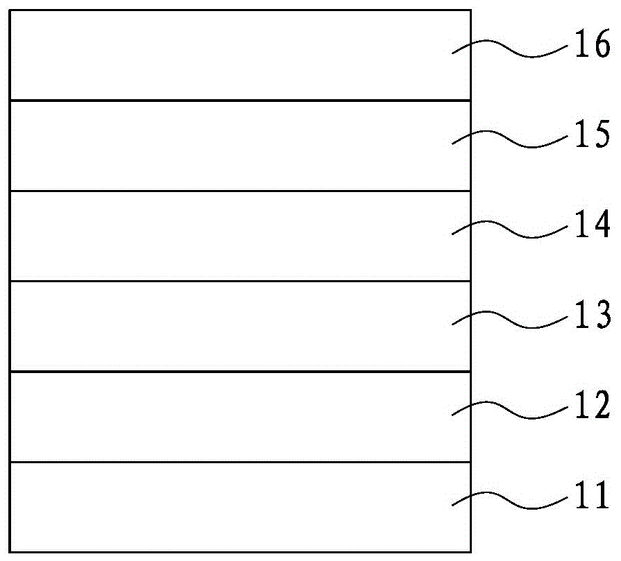
[0085] 1. On the epitaxial substrate 11, the peeling layer 12, the light-transmitting channel fabrication layer 13, the first-type conductive layer 14, the active layer 15, and the second-type conductive layer 16 are respectively epitaxially formed in sequence, such as figure 1 shown.

[0086] Wherein, the epitaxial substrate 11 is a GaAs substrate with a thickness of 300 μm. The peeling layer 12 is made of (Al 0.7 Ga 0.3 ) 0.5 In 0.5 Composed of P-35 compounds, and the thickness is 200nm. The constituent material of the transparent channel fabrication layer 13 is Al 0.4 Ga 0.6 As III-V compound, the thickness is 3 μm. The first-type conductive layer 14 is composed of a first-type rough layer, a first-type current spreading layer, and a first-type confinement layer. Among them, the first type of coarsening layer consist...

Embodiment 2

[0097] The invention discloses a method for manufacturing a light-emitting diode with electrode light output, and the specific steps are as follows:

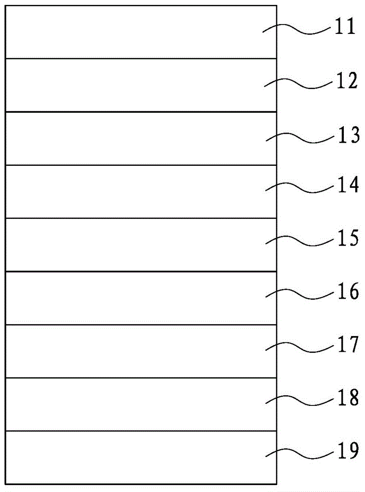
[0098] 1. On the epitaxial substrate 21, a buffer layer 22, a first-type conductive layer 23, an active layer 24, and a second-type conductive layer 25 are respectively epitaxially formed in sequence, such as Figure 7 shown.

[0099] Wherein, the epitaxial substrate 21 is a sapphire substrate with a thickness of 300 μm. The buffer layer 22 is made of undoped GaN III-V compound with a thickness of 2 μm. The first-type conductive layer 23 is made of Si-doped GaN III-V compound with a thickness of 2.5 μm. The active layer 24 adopts a cross-growth structure of five pairs of quantum wells and quantum barriers. Specifically, the quantum barrier is made of AlGaN III-V compound with a thickness of 12nm. The quantum well is composed of GaInN III-V compound with a thickness of 4nm. The second-type conductive layer 25 is made of Mg-d...

Embodiment 3

[0110] The invention discloses a method for manufacturing a light-emitting diode with electrode light output, and the specific steps are as follows:

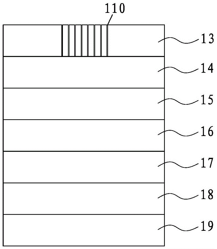
[0111] 1. On the epitaxial substrate 31, a buffer layer 32, a first-type conductive layer 33, an active layer 34, a second-type conductive layer 35, and a light-transmitting channel fabrication layer 36 are sequentially epitaxially formed, such as Figure 13 shown.

[0112] Wherein, the epitaxial substrate 31 is a GaAs substrate with a thickness of 300 μm. The first-type conductive layer 33 is composed of a Bragg reflection layer and a first-type confinement layer. Among them, the Bragg reflection layer is composed of 30 groups of Al 0.5 Ga 0.5 As / AlAs III-V compounds are alternately formed. The first-type confinement layer consists of (Al 0.7 Ga 0.3 ) 0.5 In 0.5 Composed of P-three and five-group compounds, and the thickness is 750nm. The active layer 34 is composed of 26 groups (Al 0.7 Ga 0.3 ) 0.5 In 0.5 P / Ga 0....


PUM


Abstract

The invention discloses a method for manufacturing a light-emitting diode emitting light through an electrode. According to the method, an epitaxy light-emitting structure is formed on an epitaxy of an epitaxy substrate, and a light-pervious channel manufacturing layer is formed on the epitaxy light-emitting structure; a plurality of regular light-pervious channels are formed in an electrode area of the light-pervious channel manufacturing layer by means of a mask and an ICP etching process, and the depth of the portion, undergoing ICP etching, of an electrode area allows the surface of the epitaxy light-emitting structure to be exposed; light-pervious materials are evaporated on the surface of the exposed surface of the epitaxy light-emitting structure until the light-pervious channels are filled with the materials and a light-pervious column is formed; the light-pervious channel manufacturing layer is corroded and removed, the light-pervious column is retained and the epitaxy light-emitting structure is exposed; a soldering station electrode is formed on the surface of the epitaxy light-emitting structure, and the thickness of the solder station electrode is larger than the height of the light-pervious column; the surface of a first electrode or a second electrode which serves as the soldering station electrode is under ICP etching until the upper surface of the light-pervious column is exposed; a back electrode is formed on the epitaxy light-emitting structure, and a light-emitting diode chip is formed on a split sheet. The light blocking area of the soldering station electrode can be reduced, and external quantum efficiency of the light-emitting diode can be improved.

Description

technical field [0001] The technical field of light-emitting diodes of the present invention, in particular, refers to a method for manufacturing a light-emitting diode with light-emitting electrodes. Background technique [0002] Light-emitting diodes have the advantages of low power consumption, small size and high reliability. As the main light source, they have been developed rapidly. In recent years, the application fields of light-emitting diodes have expanded rapidly, and improving the brightness of light-emitting diodes has become a key factor. [0003] In the prior art, light-emitting diodes with a multiple quantum well (MQW) structure as the active layer can obtain higher internal quantum efficiency; while the improvement of the external quantum efficiency of light-emitting diodes mainly focuses on surface roughening, metal reflection mirror technology, graphics substrate, etc. [0004] However, soldering station electrodes are basically arranged on the top of the...

Claims


Application Information

Patent Timeline
Patent Type & Authority Patents(China)
IPC IPC(8): H01L33/42H01L33/00
CPCH01L33/0062H01L33/38H01L33/42H01L2933/0016
Inventor 林志伟陈凯轩张永卓祥景姜伟杨凯蔡建九白继锋刘碧霞
Owner XIAMEN CHANGELIGHT CO LTD
Why Eureka
Try Eureka