Array substrate, manufacturing method of array substrate, flat panel detector and imaging device

A technology of array substrate and manufacturing method, which is applied in the direction of electric solid-state devices, semiconductor devices, radiation control devices, etc., and can solve the problems of reducing the detection effect of flat-panel detectors and the decline of TFT conduction performance, etc.

Active Publication Date: 2017-08-29
BOE TECH GRP CO LTD +1
View PDF5 Cites 10 Cited by
  • Summary
  • Abstract
  • Description
  • Claims
  • Application Information

AI Technical Summary

Problems solved by technology

[0003] In the prior art, when the above-mentioned photoelectric converter 101 is manufactured, it will affect the TFT on the array s

Method used


Image

  • Array substrate, manufacturing method of array substrate, flat panel detector and imaging device
  • Array substrate, manufacturing method of array substrate, flat panel detector and imaging device
  • Array substrate, manufacturing method of array substrate, flat panel detector and imaging device

Examples


Example Embodiment

[0033] The technical solutions in the embodiments of the present invention will be clearly and completely described below in conjunction with the accompanying drawings in the embodiments of the present invention. Obviously, the described embodiments are only a part of the embodiments of the present invention, rather than all the embodiments. Based on the embodiments of the present invention, all other embodiments obtained by those of ordinary skill in the art without creative work shall fall within the protection scope of the present invention.
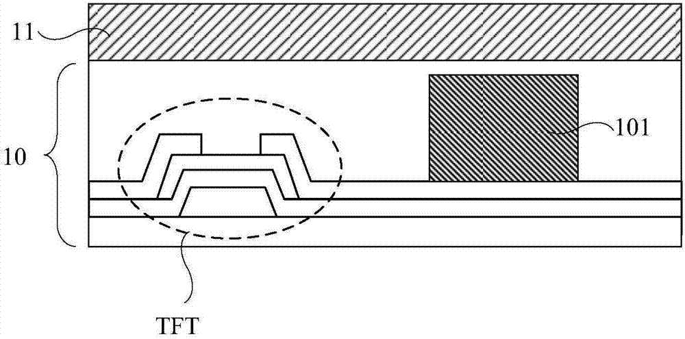
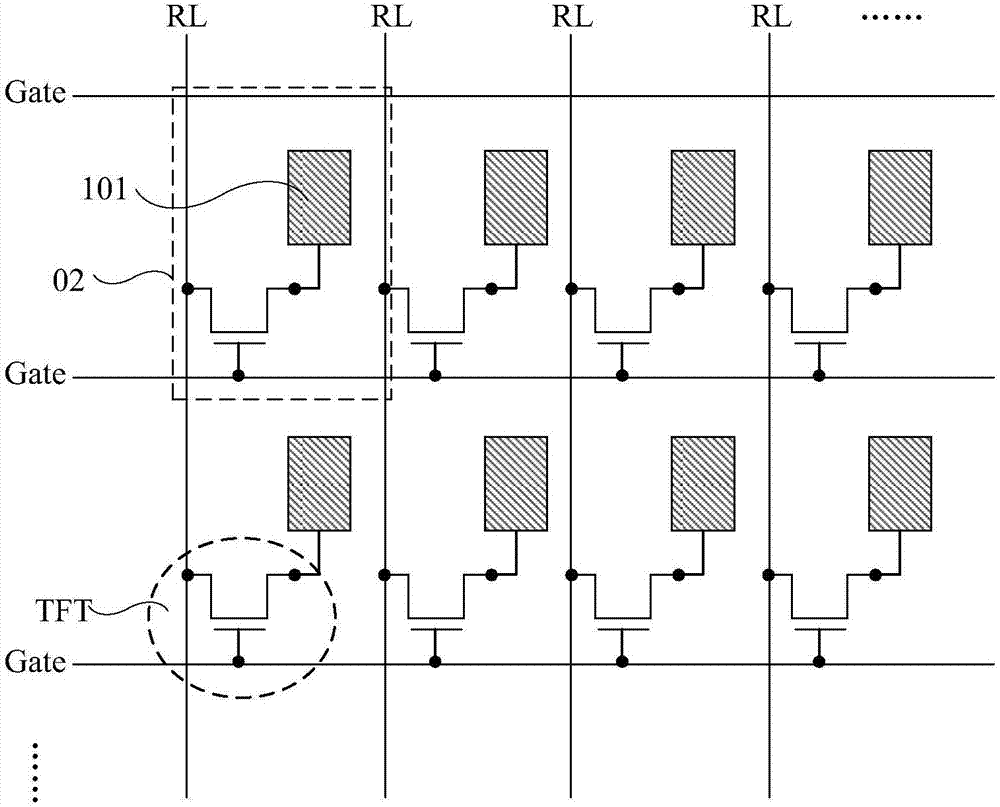
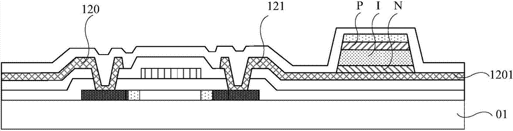
[0034] The application provides an array substrate 10, including image 3 The base substrate 01 shown is set on the base substrate 01 as figure 2 A plurality of Low Temperature Poly-Silicon (LTPS) TFTs arranged in a matrix are shown, and a photoelectric converter 101 connected to the source 120 (or drain 121) or the drain 121 of the TFT.

[0035] Wherein, the above-mentioned array substrate 10 further includes a plurality of gate lines and...


PUM


Abstract

The invention provides an array substrate, a manufacturing method of the array substrate, a flat panel detector and an imaging device, and relates to the field of photoelectric technology. The influence of manufacturing process of a photoelectric converter on the TFT performance can be reduced. The array substrate comprises a substrate, a plurality of low-temperature polycrystalline silicon TFT arranged on the substrate in an array, and a photoelectric converter connected with source electrodes or drain electrodes of the TFT, wherein the source electrode or the drain electrode of each TFT comprises a first conducting layer close to one side of the photoelectric converter, and the material constituting the first conducting layer is corrosion resistant in a composition process of the photoelectric converter. The array substrate is used for preparing the flat panel detector.

Description

technical field [0001] The invention relates to the field of optoelectronic technology, in particular to an array substrate and a manufacturing method thereof, a flat panel detector and an imaging device. Background technique [0002] X-ray detection is widely used in the medical field, and flat panel technology is usually used to detect the X-rays passing through the target to be measured. The flat panel detection technology includes direct detection and indirect detection. Among them, the Flat Panel Detector (FPD) used to realize indirect detection, such as figure 1 As shown, it includes an array substrate 10 and an X-ray conversion layer 11 covering the array substrate. Thin Film Transistors (Thin Film Transistor, TFT) and photoelectric converters 101 arranged in an array are arranged on the array substrate. The X-ray conversion layer 11 converts X-rays into visible light, and then the photoelectric converter 101 converts the visible light into electrical signals and s...

Claims


Application Information

Patent Timeline
IPC IPC(8): H01L27/12H01L27/144H01L27/146H01L21/77
CPCH01L27/124H01L27/1288H01L27/1443H01L27/14658H01L27/14683H01L27/14632H01L27/14687H01L27/14663H01L27/14616H01L27/14692
Inventor 蒋会刚高建剑郭海波朱孝会
Owner BOE TECH GRP CO LTD
Why Eureka
Try Eureka