
A kind of in-situ doping method for preparing semiconductor single crystal material by pvt method

A single crystal material, in-situ doping technology, applied in the field of in-situ doping, can solve the problems of increased process complexity, expensive equipment, crystal structure damage, etc., to achieve large-scale production, reduce crystal structure loss, uniform The effect of electrical properties

Active Publication Date: 2017-06-16
CHINA ELECTRONICS TECH GRP NO 46 RES INST
View PDF4 Cites 0 Cited by
  • Summary
  • Abstract
  • Description
  • Claims
  • Application Information

AI Technical Summary

Problems solved by technology

[0003] Under normal circumstances, the electrical properties of intrinsic semiconductor materials cannot meet the requirements of device use. In order to adjust and control the electrical properties of semiconductors, after the PVT preparation process of semiconductor single crystal materials is completed, specific elements are often diffused or ion implanted. Doped into the semiconductor material body to obtain the semiconductor single crystal material with the required electrical properties. Among them, the semiconductor material prepared by the diffusion process has obvious changes in the diffusion concentration with the depth, and its electrical uniformity is not good, and the control accuracy of the process is high. However, the ion implantation process equipment is expensive and complicated. During the implantation process, the collision of incident ions can easily cause damage to the crystal structure. Therefore, an annealing process must be added to repair the crystal structure.
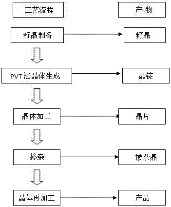
[0004] In short, the traditional PVT method to prepare semiconductor single crystal materials independently realizes the growth process and doping process of semiconductor single crystal materials, which increases the complexity of the process. At the same time, the doping process has poor doping uniformity and easily causes damage to the crystal structure. And other issues

Method used


Image

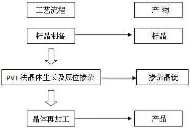
  • A kind of in-situ doping method for preparing semiconductor single crystal material by pvt method
  • A kind of in-situ doping method for preparing semiconductor single crystal material by pvt method
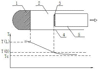
  • A kind of in-situ doping method for preparing semiconductor single crystal material by pvt method

Examples


example 1

[0012] Indium-doped N-type low-resistance cadmium sulfide single crystal was prepared by PVT method.

[0013] The growth of cadmium sulfide single crystal adopts PVT crystal growth furnace with two temperature zones. The temperature zones from the raw material end to the substrate end are respectively the first temperature zone and the second temperature zone. The quartz single crystal material is used as the substrate and the indium simple substance is used as the doping source. The elemental indium is mixed with cadmium sulfide source powder in powder state and placed in the raw material area 1. The temperature area during crystal growth is set at 1000°C and 960°C. After the growth process is completed, the growth tube is taken out, and the N-type low temperature crystal doped with indium element can be obtained. single crystal cadmium sulfide.

example 2

[0015] Chlorine-doped N-type low-resistance cadmium sulfide single crystals were prepared by PVT method.

[0016] Cadmium sulfide single crystal growth adopts PVT crystal growth furnace with two temperature zones. The temperature zones from the raw material end to the substrate end are respectively one temperature zone and two temperature zones. Quartz single crystal material is used as the substrate and cadmium chloride is used as the doping source , cadmium chloride is mixed with cadmium sulfide source powder in powder state and placed in raw material zone 1, the temperature zone during crystal growth is set to 1010°C and 980°C, after the growth process is completed, the growth tube is taken out to obtain chlorine-doped N type low resistance cadmium sulfide single crystal.

example 3

[0018] Al-doped N-type low-resistance CdSe single crystals were prepared by PVT method.

[0019] The growth of cadmium selenide single crystal adopts PVT crystal growth furnace with two temperature zones. The temperature zones from the raw material end to the substrate end are respectively the first temperature zone and the second temperature zone. The quartz single crystal material is used as the substrate and the aluminum element is used as the doping source. The elemental aluminum is mixed with cadmium selenide source powder in powder state and placed in the raw material area 1. The temperature area during crystal growth is set to 950 ° C and 900 ° C. After the growth process is completed, the growth tube is taken out to obtain aluminum-doped N type low resistance cadmium selenide single crystal.


PUM


Abstract

The invention relates to an in-situ doping method for preparing a semiconductor monocrystal material by a physical vapor transport (PVT) method. The in-situ doping method includes the following steps that (1) a double-temperature-area PVT crystal growing furnace is used, raw materials and dopants are subjected to technical processing and mixed to be together put in a raw material area, and a substrate is put at a substrate position; (2) temperatures of a first temperature area and a second temperature area of the PVT crystal growing furnace are adjusted, and the temperature range of the double temperature areas is determined according to physical properties and features of the raw materials; (3) after a growing process is finished, a growing tube is taken out, and a monocrystal doped with elements can be obtained. The in-situ doping method for preparing the semiconductor monocrystal material by the PVT method has the advantages that uniform distribution of doped elements is facilitated, uniform electrical property of the monocrystal material can be achieved, loss of a crystal structure is reduced, thereby, crystal qualities can be effectively improved, the preparation process of the monocrystal material can be simplified, and large-scale production of the monocrystal material is facilitated.

Description

technical field [0001] The invention relates to a doping method for preparing a semiconductor single crystal material by a PVT method, in particular to an in-situ doping method for preparing a semiconductor single crystal material by a PVT method. Background technique [0002] The process of preparing semiconductor single crystal material by physical vapor transport method (PVT method) is a sublimation and desublimation process, and it is also a transport process of heat, mass and power. By adjusting the temperature field distribution of single crystal furnace, growth pressure, carrier gas flow rate, etc. parameters, reduce internal defects and impurity elements, and finally prepare high-quality semiconductor single crystal materials. [0003] Under normal circumstances, the electrical properties of intrinsic semiconductor materials cannot meet the requirements of device use. In order to adjust and control the electrical properties of semiconductors, after the PVT preparatio...

Claims


Application Information

Patent Timeline
Patent Type & Authority Patents(China)
IPC IPC(8): C30B31/02C30B29/50
Inventor 张颖武程红娟练小正张志鹏李璐杰司华青徐永宽
Owner CHINA ELECTRONICS TECH GRP NO 46 RES INST
Learn More