Manufacturing method of precisely-aligned bridged-grain polysilicon thin film transistor

A technology of polysilicon thin film and manufacturing method, which is applied in the direction of transistor, semiconductor/solid-state device manufacturing, semiconductor device, etc., to achieve the effects of precise alignment, simplified process, and uniform electrical characteristics

Inactive Publication Date: 2014-04-30
GUANGDONG SINODISPLAY TECH
View PDF3 Cites 0 Cited by
  • Summary
  • Abstract
  • Description
  • Claims
  • Application Information

AI Technical Summary

Problems solved by technology

As for the conventional low-temperature polysilicon film 1101, there are severe defects in the grain boundaries 1103, such as Figure 1b shown in

Method used


Image

  • Manufacturing method of precisely-aligned bridged-grain polysilicon thin film transistor
  • Manufacturing method of precisely-aligned bridged-grain polysilicon thin film transistor
  • Manufacturing method of precisely-aligned bridged-grain polysilicon thin film transistor

Examples


Embodiment 1

[0035] This embodiment provides a method for manufacturing a bridged grain polysilicon thin film transistor, such as Figure 4a-4c Shown, including:

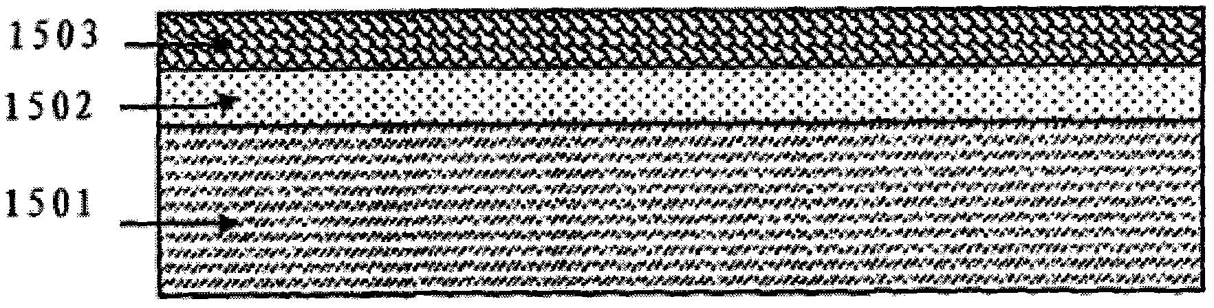
[0036] 1) Deposit a layer of low temperature oxide (LTO) on the glass substrate 101 as the barrier layer 102, and form a polysilicon layer 103 on the barrier layer 102;

[0037] 2) Etching the polysilicon layer 103 into isolated silicon islands;

[0038] 3) Using LPCVD (low pressure chemical vapor deposition) method to directly deposit the LTO gate insulating layer 201 on the polysilicon layer 103;

[0039] 4) Depositing 200 nm of low-temperature polysilicon on the gate insulating layer 201 as the gate layer 301;

[0040] 5) Coating a 1 micron positive photoresist 401 for etching on the gate layer 301;

[0041] 6), such as Figure 4a As shown, a grayscale photolithography mask is used for exposure. The grayscale photolithography mask includes light-transmitting areas 701 on both sides, and alternately arranged opaque areas 702 and partiall...

Embodiment 2

[0048] This embodiment provides a method for manufacturing a bridged grain polysilicon thin film transistor, such as Figure 4a , 4b , 5a, 5b, including:

[0049] 1), such as Figure 4a As shown, a layer of low temperature oxide (LTO) is deposited on the glass substrate 101 as the barrier layer 102, and a polysilicon layer 103 is formed on the barrier layer 102;

[0050] 2) Etching the polysilicon layer 103 into isolated silicon islands;

[0051] 3) Using LPCVD (low pressure chemical vapor deposition) method to directly deposit the LTO gate insulating layer 201 on the polysilicon layer 103;

[0052] 4) Depositing 200 nm of low-temperature polysilicon on the gate insulating layer 201 as the gate layer 301;

[0053] 5) Coating a 1 micron positive photoresist 401 for etching on the gate layer 301;

[0054] 6), such as Figure 4a As shown, a grayscale photolithography mask is used for exposure. The grayscale photolithography mask includes light-transmitting areas 701 on both sides and altern...

Embodiment 3

[0062] This embodiment provides a method for manufacturing a bridged grain polysilicon thin film transistor, such as Figure 6a-6c Shown, including:

[0063] 1) Deposit a layer of low temperature oxide (LTO) on the glass substrate 101 as the barrier layer 102, and form a polysilicon layer 103 on the barrier layer 102;

[0064] 2) Etching the polysilicon layer 103 into isolated silicon islands;

[0065] 3) Using LPCVD (low pressure chemical vapor deposition) method to directly deposit the LTO gate insulating layer 201 on the polysilicon layer 103;

[0066] 4) Depositing 200 nm of low-temperature polysilicon on the gate insulating layer 201 as the gate layer 301;

[0067] 5) Coating a 1 micron positive photoresist 401 for etching on the gate layer 301;

[0068] 6), such as Figure 6a As shown, a photolithography mask is used for exposure. The photolithography mask includes fully transparent regions 701 on both sides and alternately arranged non-transmissive regions 702 and fully transparen...


PUM


Abstract

The invention provides a manufacturing method of a precisely-aligned bridged-grain polysilicon thin film transistor. The manufacturing method includes the following steps that: 1) a polysilicon layer is formed on a substrate; 2) a gate insulating layer, a gate layer and a photoresist are formed on the polysilicon layer; 3) a gray-scale photo-etching mask plate is adopted to expose the photoresist such that a gate mask can be formed, wherein the gray-scale photo-etching mask plate comprises light-transmitting areas at two sides as well as light tight areas and partial light-transmitting areas which are located between the light-transmitting areas and are arranged alternately, wherein the light-transmitting areas at the two sides are adjacent to the light tight areas, and portions in the gate mask, which are corresponding to the partial light-transmitting areas, form grooves, and the depth of the grooves is smaller than the total thickness of the gate mask; and 4), with the gate mask adopted as a barrier, etching is performed, such that a gate can be formed, and ion implantation is performed such that the polysilicon layer can be doped, and therefore, a bridged-grain line as well as a source region and a drain region can be formed.

Description

Technical field [0001] The present invention mainly relates to polysilicon thin film transistor (TFT) technology, and more specifically, to a bridge-grain polysilicon thin film transistor that simplifies the manufacturing process while accurately aligning the gate region with the active layer region and a manufacturing method thereof. Background technique [0002] In order to realize the industrial manufacturing of polysilicon TFT active matrix display panels, high-quality polysilicon films are usually required. It needs to meet the following requirements: low-temperature processing, can be realized on a large-area glass lining, low manufacturing cost, stable manufacturing process, high performance, consistent characteristics, and high reliability of polysilicon TFT. [0003] High-temperature polysilicon technology can be used to realize high-performance TFTs, but it cannot be used for common glass substrates used in commercial display panels. In such cases, low-temperature polysi...

Claims


Application Information

Patent Timeline
Patent Type & Authority Applications(China)
IPC IPC(8): H01L21/336H01L29/786
CPCH01L29/66757H01L21/26506H01L29/78675
Inventor 黄宇华史亮亮赵淑云
Owner GUANGDONG SINODISPLAY TECH
Why Eureka
Try Eureka