Preparing method of whole back electrode P type crystalline silicon heterojunction solar battery

A technology of solar cells and full back electrodes, applied in circuits, photovoltaic power generation, electrical components, etc., can solve the problems of increasing potential barriers and reducing open circuit voltage, achieving the effects of increasing light receiving area, increasing open circuit voltage, and reducing production costs

Active Publication Date: 2014-11-26
48TH RES INST OF CHINA ELECTRONICS TECH GROUP CORP
View PDF6 Cites 10 Cited by
  • Summary
  • Abstract
  • Description
  • Claims
  • Application Information

AI Technical Summary

Problems solved by technology

The most deadly problem is that in the CN102214720A patent "the N-type region forms a p + a-si / i-a-si / P-c-si / P + "Back side P in c-si / i-a-si / n-a-si heterojunction structure" + The existence of "c-si diffused silicon layer" leads to an increase in the potential barrier, which greatly reduces the open circuit voltage, so it is necessary to remove the N-type region of the P + Diffusion layer; and the "front surface p + Amorphous silicon film / P-type silicon substrate / P-region electrode" also makes it difficult for holes to cross the potential barrier to reach the P-region electrode

Method used


Image

  • Preparing method of whole back electrode P type crystalline silicon heterojunction solar battery
  • Preparing method of whole back electrode P type crystalline silicon heterojunction solar battery
  • Preparing method of whole back electrode P type crystalline silicon heterojunction solar battery

Examples


Embodiment 1

[0048] Example 1, as Figure 1-10 As shown, a preparation method of a full-back electrode P-type crystalline silicon heterojunction solar cell includes the following steps:

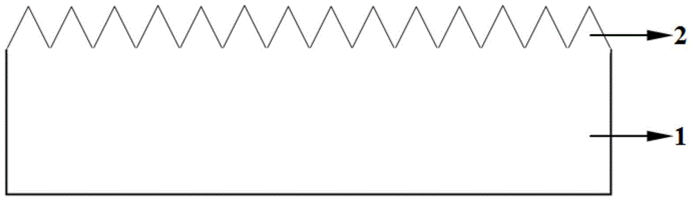
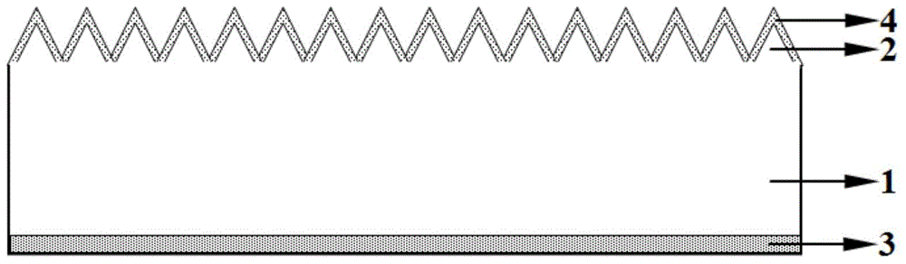
[0049] (1) Using the metal catalytic chemical etching method, a pyramid-like nano-suede surface is prepared on the front surface of the P-type silicon substrate, and the size of the nano-suede surface is 200 nm, and then the residual metal particles and other harmful substances are washed away by a cleaning process;

[0050] (2) Prepare p on the backside of p-type silicon substrate by high temperature diffusion of boron source ++ Type boron re-diffusion layer crystalline silicon layer, its thickness is 0.3μm, and the sheet resistance is 80ohm / Sq;

[0051] (3) Preparation of p on the backside of p-type silicon substrate by high-temperature shallow diffusion of boron source + Type boron shallow diffusion layer crystalline silicon layer, its thickness is 0.3μm, and the sheet resistance is 130ohm / Sq;

[00...

Embodiment 2

[0059] Example 2, as Figure 1-10 As shown, a preparation method of a full-back electrode P-type crystalline silicon heterojunction solar cell includes the following steps:

[0060] (1) Using the metal catalytic chemical etching method, a pyramid-like nano-suede surface is prepared on the front surface of the P-type silicon substrate, and the nano-suede size is 150 nm, and then the residual metal particles and other harmful substances are washed away by a cleaning process;

[0061] (2) By ion implantation, the p-type silicon substrate is prepared on the back side to obtain p ++ type boron re-diffusion layer crystalline silicon layer, its thickness is 0.2μm, and the sheet resistance is 70ohm / Sq;

[0062] (3) By ion implantation, the p-type silicon substrate is prepared on the back side to obtain p + Type boron shallow diffusion layer crystalline silicon layer, its thickness is 0.2μm, and the sheet resistance is 150ohm / Sq;

[0063] (4) By thermal oxidation method, SiOx film i...


PUM

PropertyMeasurementUnit
thicknessaaaaaaaaaa
thicknessaaaaaaaaaa
thicknessaaaaaaaaaa

Abstract

The invention discloses a preparing method of a whole back electrode P type crystalline silicon heterojunction solar battery. The method comprises the steps that nanometer suede, a P+ type boron shallow diffusion crystalline silicon layer and an SiOx passivation/SiNx anti-reflection layer are prepared on the front surface of a P type silicon substrate; a P++ type boron heavy diffusion crystalline silicon layer is prepared on the back face of the P type silicon substrate, then printing corrosion slurry is used for achieving local corrosion on the P++ type boron heavy diffusion crystalline silicon layer, an intrinsic amorphous silicon membrane layer and an n type amorphous silicon membrane layer are subjected to deposition in sequence, and intrinsic and n type amorphous silicon on the surface layer of a P++ type boron heavy diffusion crystalline silicon layer zone is removed; then a transparent conducting membrane layer is subjected to sputtering, a P zone and an N zone on the back face of the P type silicon substrate are separated through laser; and finally electrode printing is carried out, and low-temperature sintering is carried out. According to the method, all metal electrodes are moved to the back face of the battery, electrodes are not arranged on a light-borne face, component production cost is lowered, battery composite loss is lowered, accordingly, optical loss and resistance are obviously lowered, and efficiency is greatly improved.

Description

technical field [0001] The invention relates to a method for preparing a solar cell structure, in particular to a method for preparing a P-type crystalline silicon heterojunction solar cell with full back electrodes. Background technique [0002] With the continuous development of crystalline silicon solar cell technology, great achievements have been made in the research of high-efficiency monocrystalline silicon solar cell. The full back electrode (IBC) battery structure developed by Sunpower Corporation of the United States has all the grid electrodes designed to the back of the battery, and the positive and negative electrodes are arranged in a crossed manner. The mass production efficiency can reach 23%, and the highest laboratory efficiency can reach 24.2%. In April 2014, Panasonic announced that by combining heterojunction technology (HIT) and back contact electrode technology (IBC), its newly developed commercial size (143.7cm 2 ) The photoelectric conversion effici...

Claims


Application Information

Patent Timeline
Patent Type & Authority Applications(China)
IPC IPC(8): H01L31/18H01L31/0747H01L31/0224H01L31/0236
CPCH01L31/02363H01L31/0747Y02E10/50Y02P70/50
Inventor 刘文峰周洪彪程文进汪已琳
Owner 48TH RES INST OF CHINA ELECTRONICS TECH GROUP CORP
Why Eureka
Try Eureka