TFT (Thin Film Transistor) array substrate, manufacturing method thereof, and display device

A technology of an array substrate and a manufacturing method is applied in the display field to achieve the effects of eliminating light leakage, reducing the step difference and improving the display quality

Inactive Publication Date: 2015-03-04
HEFEI BOE OPTOELECTRONICS TECH +1
View PDF3 Cites 10 Cited by
  • Summary
  • Abstract
  • Description
  • Claims
  • Application Information

AI Technical Summary

Problems solved by technology

[0005] In order to overcome the defects in the above-mentioned prior art, the technical problem to be solved by the present invention is: to provide a TFT array substrate and its manufacturing method, and a display device, so as to reduce the step difference caused by the data lines, eliminate the problems of light leakage and contrast reduction, etc. , to improve display quality

Method used


Image

  • TFT (Thin Film Transistor) array substrate, manufacturing method thereof, and display device
  • TFT (Thin Film Transistor) array substrate, manufacturing method thereof, and display device
  • TFT (Thin Film Transistor) array substrate, manufacturing method thereof, and display device

Examples


Embodiment Construction

[0024] In order to make the above objects, features and advantages of the present invention more obvious and understandable, the technical solutions in the embodiments of the present invention will be clearly and completely described below in conjunction with the drawings in the embodiments of the present invention. Apparently, the described embodiments are only some of the embodiments of the present invention, but not all of them. Based on the embodiments of the present invention, all other embodiments obtained by persons of ordinary skill in the art without creative efforts fall within the protection scope of the present invention.

[0025] An embodiment of the present invention provides a method for manufacturing a TFT array substrate, including the following steps:

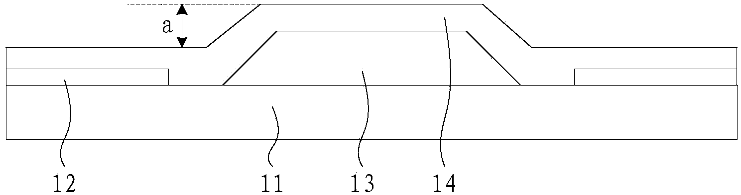
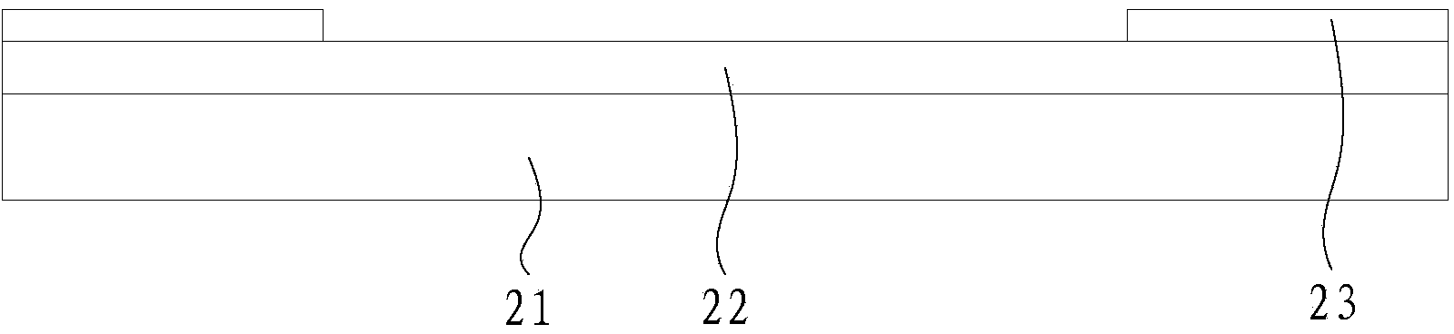
[0026] Step S1: forming a gate insulating layer 22 on the substrate 21 formed with the gate line and the active layer, such as figure 2 shown.

[0027] In this step, the material for forming the gate insula...


PUM


Abstract

The invention provides a TFT (Thin Film Transistor) array substrate, a manufacturing method thereof, and a display device. the manufacturing method comprises steps: Passivation layers are formed on a substrate provided with a data line, wherein the passivation layers comprise a first passivation layer covering the data line and a second passivation layer covering other regions expect the data line; and the first passivation layer with a first preset thickness is removed to enable the thickness of the first passivation layer to be smaller than the thickness of the second passivation layer. in the above manufacturing method, through removing a passivation layer with a certain thickness covering the data line after the passivation layers are formed so as to enable the thickness of the passivation layer covering the data line to be smaller than the thickness of the passivation layer covering other regions expect the data line, segment difference caused as the thickness of the data line is thick can be effectively reduced problems of light leak, reduced contrast ratio and the like can be eliminated, and the display quality is improved.

Description

technical field [0001] The present invention relates to the field of display technology, in particular to a TFT (Thin Film Transistor, thin film transistor) array substrate, a manufacturing method thereof, and a display device. Background technique [0002] TFT-LCD (Thin Film Transistor Liquid Crystal Display, Thin Film Transistor Liquid Crystal Display) occupies a dominant position in the flat panel display market due to its advantages of small size, low power consumption, and no radiation. With the advancement of technology, consumers have put forward higher requirements for the display effect of the display, and the pursuit of performance such as high transmittance, wide viewing angle, high aperture ratio, low color difference, and low response time has prompted the rapid development of display technology. [0003] An important part of TFT-LCD includes a TFT array substrate. The TFT array substrate has an alignment layer on the side facing the liquid crystal. The process ...

Claims


Application Information

Patent Timeline
Patent Type & Authority Applications(China)
IPC IPC(8): H01L21/3105H01L21/82H01L27/02
CPCH01L21/77H01L27/1248H01L27/1259H01L2021/775H01L27/124H01L27/1288
Inventor 罗强强杨玖娟
Owner HEFEI BOE OPTOELECTRONICS TECH
Why Eureka
Try Eureka