Impact-resistant packaging structure of multi-chip integrated circuit

An integrated circuit and packaging structure technology, applied in circuits, electrical components, electrical solid devices, etc., can solve problems such as easily damaged wire bonds and chip surfaces, prevent extrusion effects and temperature stress effects, and improve assembly reliability. Effect

Inactive Publication Date: 2015-03-04
EAST CHINA INST OF OPTOELECTRONICS INTEGRATEDDEVICE
View PDF14 Cites 4 Cited by
  • Summary
  • Abstract
  • Description
  • Claims
  • Application Information

AI Technical Summary

Problems solved by technology

[0003] The purpose of the present invention is to solve the shortcomings of the existing integral hard material potting structure of integrated circuits, which is easy to damage the wire bonding and chip surface under the action of environmental stress, and to provide a multi-chip integrated circuit impact-resistant packaging structure

Method used


Image

  • Impact-resistant packaging structure of multi-chip integrated circuit
  • Impact-resistant packaging structure of multi-chip integrated circuit

Examples


Embodiment Construction

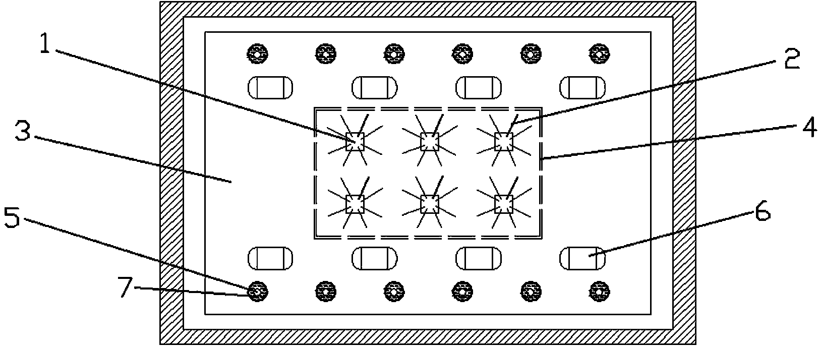
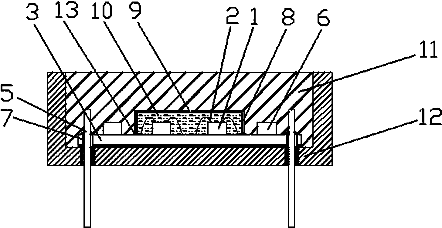
[0016] (1) If figure 1 As shown, the bonding area of ​​the bare chip 1 and the lead wire 2 is concentratedly arranged in the middle of the circuit substrate 3, and the cap bonding area 4 is reserved around the bonding area of ​​the bare chip. Complete the wire bonding assembly between the bare chip 1 and the substrate 3 , the assembly of the substrate 3 and the case base 12 , the electrical connection between the substrate and the case leads 5 , and the assembly of other components 6 on the substrate. Among them, the substrate 3 and the casing lead 5 adopt a conventional package interconnection method, that is, the edge of the substrate 3 is provided with a through hole, the casing lead 5 passes through the through hole, and the conductive material 7 (conductive epoxy or solder, etc.) is used on the periphery of the through hole. Enables interconnection of leads to via pads.

[0017] (2) Make the cap 8 of the box body structure, the top of the cap has a small hole 9, and the ...


PUM


Abstract

The invention relates to an impact-resistant packaging structure of a multi-chip integrated circuit. The impact-resistant packaging structure is characterized in that bare chips (1) and lead (2) bonding zones are arranged at a substrate (3) in a centralized mode and are placed inside caps (8); soft packaging materials (10) are poured into the caps (8) for sealing; and hard packaging materials (11) are poured into other parts of the integrated circuit inside a housing (12) for sealing. The impact-resistant packaging structure has the following advantages: with pouring and sealing of the soft materials inside the caps, the chips and the lead bonding units can be protected from being damaged under the environment stress, especially the temperature changing stress and the impact-resistant protection effect of the hard pouring and sealing can be realized. On the basis of the cap protection structure, the extrusion effect on the soft materials by the hard materials and the temperature stress effect can be effectively prevented and thus the chips and lead bonding zones can be further protected, thereby improving the product assembling reliability.

Description

technical field [0001] The invention relates to the technical field of integrated circuits, in particular to an impact-resistant packaging structure for multi-chip integrated circuits. Background technique [0002] Internal potting is an important means to improve the impact resistance of hybrid integrated circuits. In order to ensure the effect of potting, the overall potting of the circuit is usually made of hard materials. The purpose is to absorb and disperse the high overload of the internal substrate and components of the circuit. Impact stress to improve the overall impact resistance of the circuit. Since the overall potting is made of hard materials, this kind of potting is easy to damage the wire bonding and chip surface under the action of environmental stress (especially temperature change stress), for example, it will cause the bonding wire to break and the interconnection of the bonding point to fail, etc. , there are many bare chips in the hybrid integrated ci...

Claims


Application Information

Patent Timeline
Patent Type & Authority Applications(China)
IPC IPC(8): H01L23/31H01L23/29
CPCH01L2224/48091H01L2224/48227H01L2224/49171H01L2924/181H01L2924/19105H01L2924/00014H01L2924/00012
Inventor 夏俊生邹建安周峻霖潘大卓
Owner EAST CHINA INST OF OPTOELECTRONICS INTEGRATEDDEVICE
Why Eureka
Try Eureka