Small-sized LED lamp bead set and lamp beads

A technology of LED lamp beads and small size, which is applied in the direction of electrical components, electric solid devices, circuits, etc., which can solve the problems of poor electrical conductivity of products, huge process difficulty, and poor copper plating effect, so as to reduce density and process Difficulty, the effect of reducing the number of vias

Inactive Publication Date: 2015-03-11
MLS
View PDF6 Cites 2 Cited by
  • Summary
  • Abstract
  • Description
  • Claims
  • Application Information

AI Technical Summary

Problems solved by technology

However, there are still many difficulties in this technology: (1) Since an LED lamp bead needs to have multiple pins, especially colorful LED lamp beads, it includes more pins, and in this technology each Each pin needs to start a through hole to connect the pin to the upper copper foil of the bracket. When an LED lamp bead requires multiple pins, it means opening multiple through holes on the bracket, and as mentioned above Yes, the size of the bracket is very small, opening multiple through holes on such a small size at the same time, resulting in a high density of perforating needles, which is extremely difficult in the process
(2) Due to the very small size of the bracket, when multiple through holes need to be opened, the aperture of the through holes must be appropriately reduced, and the through holes with small apertures will easily lead to poor copper plating effect, resulting in poor electrical conductivity of the product

Method used


Image

  • Small-sized LED lamp bead set and lamp beads
  • Small-sized LED lamp bead set and lamp beads
  • Small-sized LED lamp bead set and lamp beads

Examples


Embodiment Construction

[0024] The present invention is further described in conjunction with the following examples.

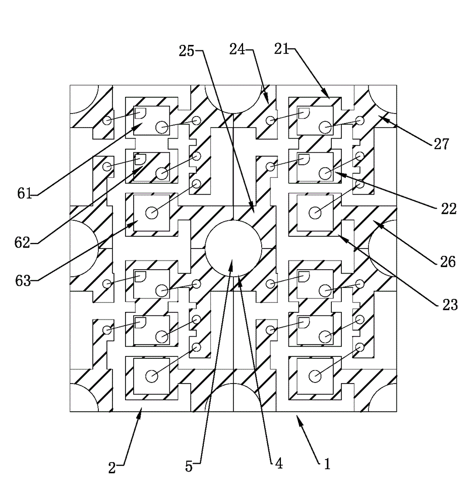
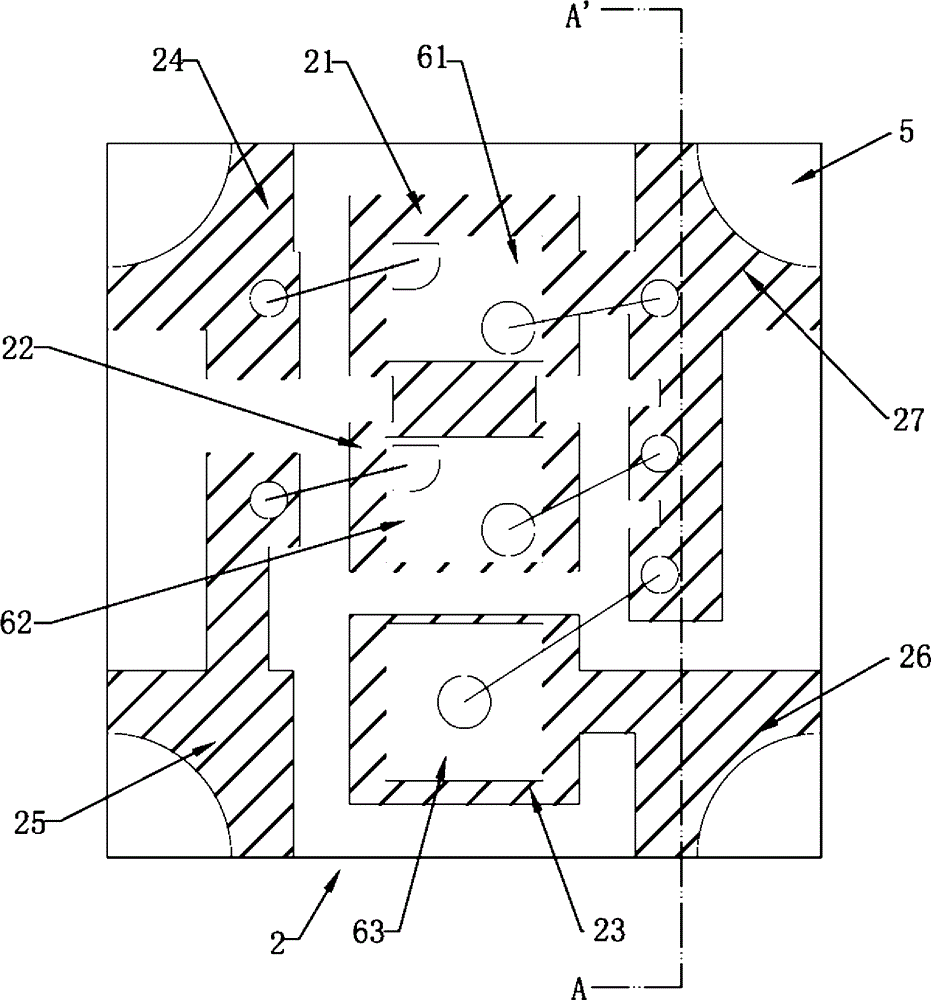
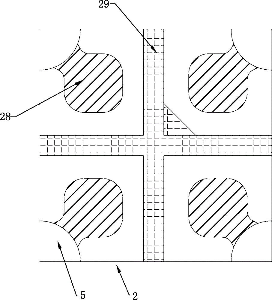
[0025] The present invention creates a specific embodiment of a small-sized LED lamp bead group, such as Figure 1 to Figure 3 As shown, it includes a bracket group and LED crystals fixed on the bracket group. The LED crystal includes a blue crystal 1, a green crystal 62 and a red crystal 63. The bracket group includes a square resin substrate 1 with a black upper surface. The resin substrate 1 Divide a plurality of quadrangular support substrates 2 (for ease of illustration, only four are shown in the figure), so that four adjacent quadrangular support substrates 2 share a vertex, and the front of each support substrate 2 is provided with roughly a The three crystal-bonding copper foils used to fix the LED crystal in a word arrangement are B crystal-bonding copper foil 21 for fixing blue light crystal 1, G crystal-bonding copper foil 22 for fixing green light crystal 62, and G crys...


PUM

PropertyMeasurementUnit
Roughnessaaaaaaaaaa

Abstract

The invention creatively provides a small-sized LED lamp bead set and lamp beads formed by cutting the lamp bead set. A bracket set forming the lamp bead set is formed by splicing a plurality of brackets; the brackets share a top point, and a through hole is formed in the top point shared by the brackets and used for allowing a conductive layer to be plated in, so that one conductive through hole can be shared by the brackets, the number of required through holes is effectively reduced, and the density of the through holes is reduced; moreover, the apertures of the through holes can be set to be relatively large, so that the process difficulty can be effectively lowered and the product yield can be increased.

Description

technical field [0001] The invention relates to the technical field of LED packaging, in particular to a small-sized LED lamp bead group and lamp beads. Background technique [0002] With the development of technology, the pixels of LED display screens are getting higher and higher, and the pixels are becoming more and more dense, which requires that the size of the LED lamp beads that make up the pixels must be very small, which has greatly improved the LED packaging technology. high demands. In the packaging technology, the core is the structure of the bracket, which determines the size and packaging structure of the final LED lamp bead. The bracket of the traditional patch type LED lamp bead is formed by injection molding on the metal bracket. The bracket protrudes metal pins to both sides. Obviously, the protruding pins to both sides will occupy part of the space, resulting in a large distance between adjacent LEDs. [0003] In this regard, the double-layer PCB board t...

Claims


Application Information

Patent Timeline
IPC IPC(8): H01L33/62H01L33/48
CPCH01L2224/48227
Inventor 刘天明皮保清肖虎张沛涂梅仙
Owner MLS
Why Eureka
Try Eureka