
Manufacturing method of yin-yang copper-thickness printed circuit board

A technology for printed circuit boards and manufacturing methods, which is applied in the fields of printed circuit manufacturing, printed circuits, and removal of conductive materials by chemical/electrolytic methods, and can solve problems such as inability to process fine lines

Inactive Publication Date: 2015-03-18
SHENZHEN SUNTAK MULTILAYER PCB
View PDF4 Cites 12 Cited by
  • Summary
  • Abstract
  • Description
  • Claims
  • Application Information

AI Technical Summary

Problems solved by technology

[0004] The purpose of the present invention is to provide a method for manufacturing a yin-yang copper thick printed circuit board, which adopts separate etching treatment on the thick copper surface and the thin copper surface, aiming to solve the problem that the fine circuit cannot be processed in the prior art

Method used


Image

  • Manufacturing method of yin-yang copper-thickness printed circuit board
  • Manufacturing method of yin-yang copper-thickness printed circuit board

Examples


Embodiment Construction

[0048] In order to make the object, technical solution and advantages of the present invention clearer, the present invention will be further described in detail below in conjunction with the accompanying drawings and embodiments. It should be understood that the specific embodiments described here are only used to explain the present invention, not to limit the present invention.

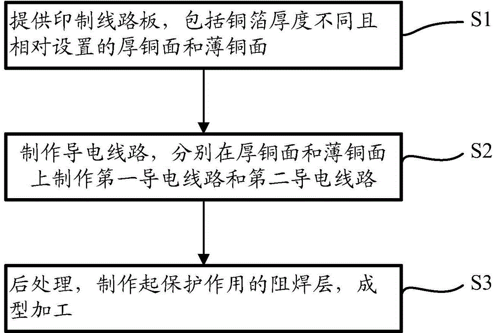
[0049] Please parameter figure 1 with figure 2 , the manufacturing method of the yin-yang copper thick printed wiring board provided by the embodiment of the present invention comprises the following steps:

[0050] S1: Provide a printed circuit board, the printed circuit board includes a thick copper surface and a thin copper surface with different copper foil thicknesses and are arranged oppositely; it can be understood that the thick copper surface and the thin copper surface in this embodiment are relative concepts .

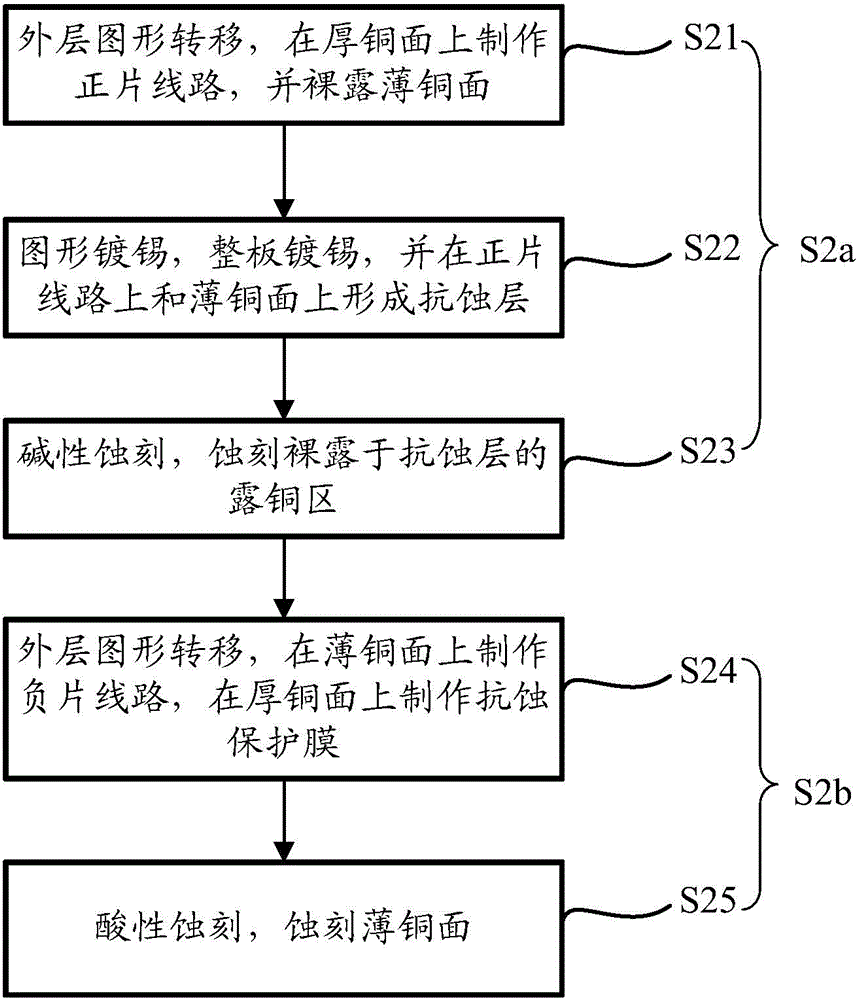
[0051] S2: making a conductive circuit, respectively making a first cond...


PUM


Abstract

The invention is applicable to the technical field of processing of a printed circuit board and provides a manufacturing method of a yin-yang copper-thickness printed circuit board. Separate etching processing of a thick copper surface and a thin copper surface is adopted so as to solve a problem of incapability of processing fine lines in the prior art. The manufacturing method includes the following steps: providing a printed circuit board with different copper foil thicknesses; manufacturing conductive lines: manufacturing a first conductive line and a second conductive line on a thick copper surface and a thin copper surface respectively; and post-processing. The step of manufacturing the first conductive line on the thick copper surface includes the following steps: outer-layer pattern transference, pattern tinning and alkaline etching. The step of manufacturing the second conductive line on the thin copper surface includes the following steps: outer-layer pattern transference and alkaline etching. In the method, the first conductive pattern and the second conductive pattern are manufactured on the thick copper surface and the thin copper surface respectively so as to manufacture fine lines on the printed circuit board with different copper foil thicknesses so that the manufacturing method is suitable for processing a printed circuit board, in which the range of copper foil thicknesses of two surfaces is an any value.

Description

technical field [0001] The invention belongs to the technical field of printed circuit board processing, and in particular relates to a method for manufacturing a yin-yang copper thick printed circuit board. Background technique [0002] In the manufacture of printed circuit boards, the etching process is an indispensable and important step. Especially with the rapid development of microelectronics technology and the wide application of large-scale integrated circuits and ultra-large-scale integrated circuits, the width and spacing of wires on printed circuit boards are getting smaller and smaller, and the wiring density and precision are getting higher and higher. Higher and stricter technical requirements are put forward for the precision and tolerance of etching, and the quality of etching directly affects the quality of printed circuit boards. [0003] For printed circuit boards with the same thickness of copper foil, usually, simultaneous etching on both sides can meet...

Claims


Application Information

Patent Timeline
Patent Type & Authority Applications(China)
IPC IPC(8): H05K3/06
CPCH05K3/061H05K2203/1476
Inventor 常文智刘东吴甲林韩启龙
Owner SHENZHEN SUNTAK MULTILAYER PCB
Features
  • Generate Ideas
  • Intellectual Property
  • Life Sciences
  • Materials
  • Tech Scout
  • Unparalleled Data Quality
  • Higher Quality Content
  • 60% Fewer Hallucinations
Learn More