Manufacturing method of low temperature poly-silicon thin film transistor

A technology of low-temperature polysilicon and thin-film transistors, applied in the direction of transistors, semiconductor/solid-state device manufacturing, semiconductor devices, etc., can solve problems such as inability to increase thickness, poor bright spots, and complicated manufacturing process of TFT substrates, so as to reduce consumption and reduce poor bright spots. Effect

Inactive Publication Date: 2019-04-12
WUHAN CHINA STAR OPTOELECTRONICS SEMICON DISPLAY TECH CO LTD
View PDF2 Cites 4 Cited by
  • Summary
  • Abstract
  • Description
  • Claims
  • Application Information

AI Technical Summary

Problems solved by technology

However, the manufacturing process of the TFT substrate in the LTPS display panel is very complicated. In the existing technology, when the low-temperature polysilicon semiconductor layer is heavily doped with ions and lightly doped with ions, the doped ions need to penetrate the gate insulating layer to reach the low-temperature polysilicon. The semiconductor layer, which leads to a large consumption of doping materials during doping, and the gate insulating layer is limited by the ion implantation ability, and the thickness cannot be increased. The thinner gate insulating layer is susceptible to film formation conditions and environmental impurities (Particle) effect, resulting in bad bright spots

Method used


Image

  • Manufacturing method of low temperature poly-silicon thin film transistor
  • Manufacturing method of low temperature poly-silicon thin film transistor
  • Manufacturing method of low temperature poly-silicon thin film transistor

Examples


Embodiment Construction

[0038] In order to further illustrate the technical means adopted by the present invention and its effects, the following describes in detail in conjunction with preferred embodiments of the present invention and accompanying drawings.

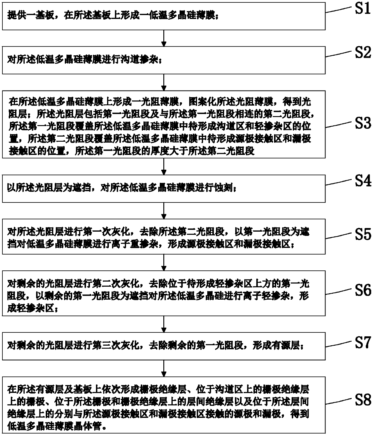
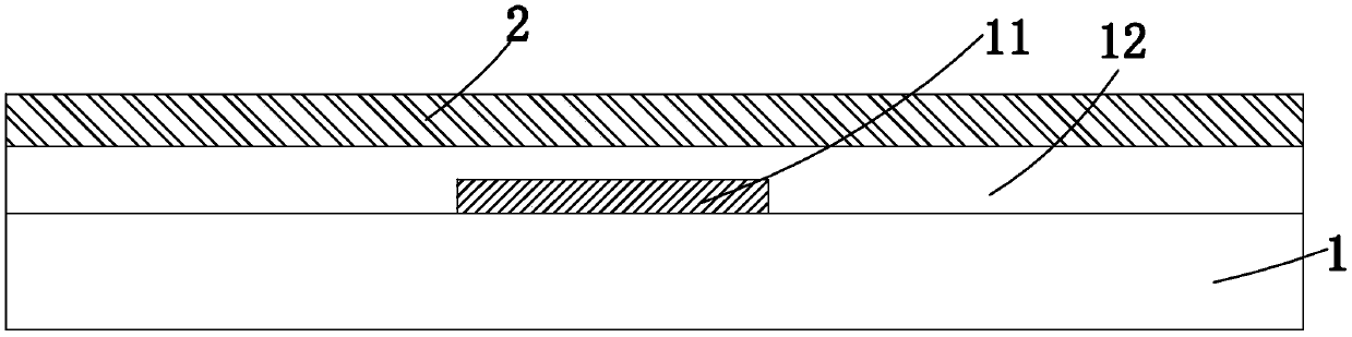
[0039] see figure 1 , the invention provides a method for manufacturing a low-temperature polysilicon thin film transistor, comprising the steps of:

[0040] Step S1 , providing a substrate 1 , and forming a low temperature polysilicon film 2 on the substrate 1 .

[0041] Specifically, the substrate 1 is a transparent substrate, preferably a glass substrate.

[0042] Specifically, before forming the low-temperature polysilicon thin film 2 in the step S1, it also includes the steps of forming a light-shielding layer 11 on the substrate 1 and forming a buffer layer 12 on the light-shielding layer 11 and the substrate 1. The low-temperature polysilicon thin film 2 is formed on the buffer layer 12.

[0043] Specifically, the step of forming the...


PUM


Abstract

The invention provides a manufacturing method of a low temperature poly-silicon thin film transistor. According to the method, before a gate insulating layer is formed, a photoresist layer with a first photoresist section and a second photoresist section with different thicknesses is formed on a low temperature poly-silicon thin film firstly; then by matching with multiple ashing processes, an active layer which comprises a channel region, a source electrode contact region and a drain electrode contact region located on the two sides of the channel region respectively, and light doped regionslocated between the channel region and the source electrode contact region and between the channel region and the drain electrode contact region is manufactured, so that the consumption of the doped materials can be reduced; and meanwhile, the limitation on the thickness of the gate insulating layer caused by ion doping is avoided, so that the badness of bright spots is reduced.

Description

technical field [0001] The invention relates to the field of display technology, in particular to a method for manufacturing a low-temperature polysilicon thin film transistor. Background technique [0002] With the development of display technology, liquid crystal displays (Liquid Crystal Display, LCD) and other flat display devices are widely used in mobile phones, televisions, personal Various consumer electronic products such as digital assistants, digital cameras, notebook computers, and desktop computers have become the mainstream of display devices. [0003] Most of the liquid crystal display devices currently on the market are backlight liquid crystal displays, which include a liquid crystal display panel and a backlight module. The working principle of the liquid crystal display panel is to place liquid crystal molecules between two parallel glass substrates. There are many vertical and horizontal small wires between the two glass substrates. The direction of the l...

Claims


Application Information

Patent Timeline
Patent Type & Authority Applications(China)
IPC IPC(8): H01L21/336H01L29/786
CPCH01L29/66757H01L29/66772H01L29/78675
Inventor 胡重粮
Owner WUHAN CHINA STAR OPTOELECTRONICS SEMICON DISPLAY TECH CO LTD
Why Eureka
Try Eureka