Material defect detector and material defect detection method

A technology for material defects and detection equipment, applied in the direction of material capacitance, etc., can solve problems such as non-destructive testing of materials inside

Active Publication Date: 2015-03-25
秦皇岛光宇玻纤制品股份有限公司
View PDF7 Cites 20 Cited by
  • Summary
  • Abstract
  • Description
  • Claims
  • Application Information

AI Technical Summary

Problems solved by technology

[0004] The embodiment of the present invention provides a material defect detection device and a material defect detection method, w

Method used


Image

  • Material defect detector and material defect detection method
  • Material defect detector and material defect detection method
  • Material defect detector and material defect detection method

Examples


Embodiment 1

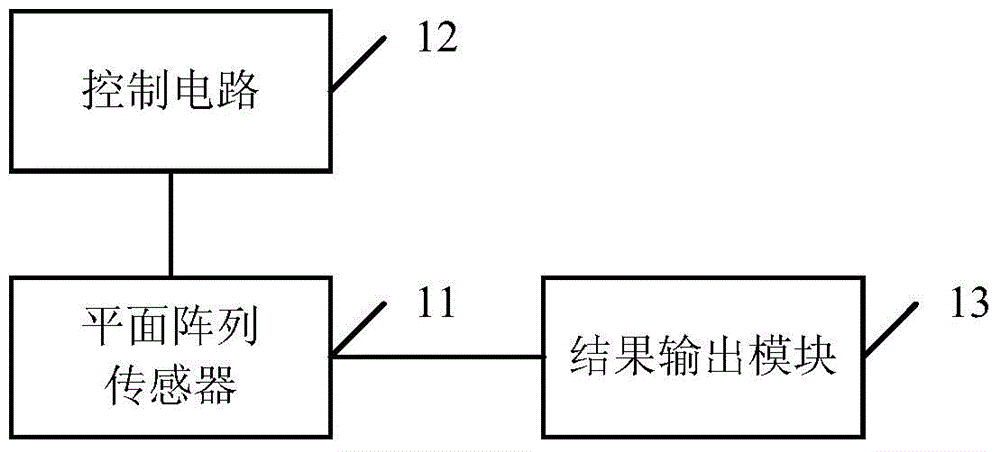
[0064] Embodiment 1 of the present invention provides a material defect detection device, such as figure 1 shown, including:

[0065] A planar array sensor 11, a control circuit 12 and a result output module 13 for detection, wherein:

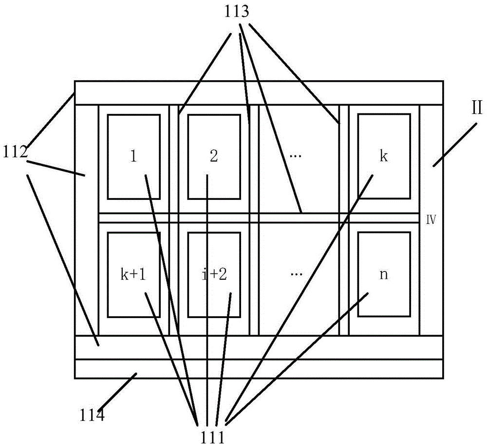
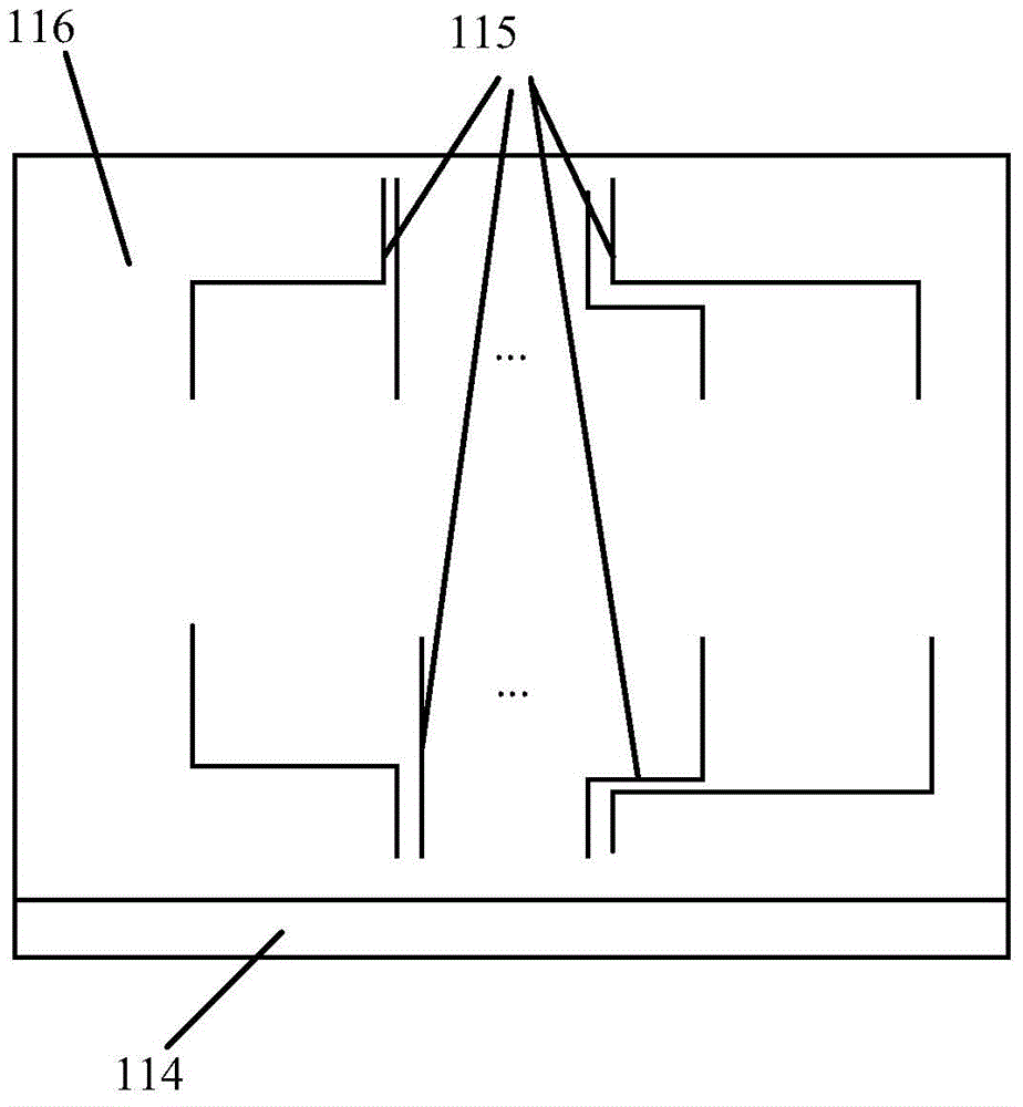
[0066] Such as Figure 2A and Figure 2B As shown, the planar array sensor includes: multiple detection electrodes 111, end shielding electrodes 112, inter-electrode shielding electrodes 113, sensor substrate 114, signal line 115 and substrate back shielding layer 116, wherein:

[0067] The control circuit 12 is connected to the plurality of detection electrodes 111, and is used to control the voltage excitation to the plurality of detection electrodes 111;

[0068] A plurality of detection electrodes 111 are arranged in an array above the sensor substrate 114, inter-electrode shielding electrodes 113 are distributed between the plurality of detection electrodes 111, end shielding electrodes 112 are distributed around the plurality of detect...

Embodiment 2

[0094] According to the same inventive concept, based on the material defect detection equipment provided in the above-mentioned embodiment 1 of the present invention, embodiment 2 of the present invention also provides a material defect detection method, such as Figure 5 shown, including:

[0095] Step 501, through the above-mentioned control circuit of the material defect detection device, sequentially perform voltage excitation on each electrode pair to be detected of the plurality of detection electrodes of the planar array sensor.

[0096] Step 502: Output a corresponding detection result according to the detection signal generated after each electrode pair to be detected is excited by the voltage.

[0097] The method provided by the present invention will be described in detail below with specific embodiments in conjunction with the accompanying drawings.

[0098] Figure 6 The detailed flowchart of the material defect detection method provided by Embodiment 2 of the ...


PUM


Abstract

The invention discloses a material defect detector and a material defect detection method. The material defect detector comprises a planar array sensor, a control circuit and a result output module, wherein the planar array sensor comprises multiple detection electrodes, an end part shielding electrode, an interstage shielding electrode, a sensor substrate, signal lines and a substrate back surface shielding layer; the control circuit is connected with the multiple detection electrodes for controlling voltage drive on the multiple detection electrodes; the multiple detection electrodes are arranged above the sensor substrate in an array manner, the substrate back surface shielding layer covers the back surface of the sensor substrate, and the signal lines are distributed on the back surface of the sensor substrate; the signal lines are connected with the multiple detection electrodes, are also connected with the result output module, are used for transmitting detection signals to the result output module; the result output module is used for outputting corresponding detection results according to the detection signals. By utilizing the scheme provided by the invention, the nondestructive testing to the interior of a material is realized.

Description

technical field [0001] The present invention relates to the technical field of material defect detection and non-destructive detection technology, in particular to a material defect detection device and a material defect detection method. Background technique [0002] In recent years, various new composite materials have played an increasingly important role in the construction of aircraft structures, and are even used in key parts related to flight safety. Among them, a new composite material with a laminated porous structure with strong sound absorption properties is the most common. The material is a fiber-reinforced metal material formed by alternate lamination and binding of high-strength aluminum sheets and high-strength glass fiber-reinforced resins, and the internal porosity is greater than 90%. During the production and use of this material, due to the influence of factors such as manual operation, environment, and external load, there will inevitably be defects su...

Claims


Application Information

Patent Timeline
IPC IPC(8): G01N27/22
Inventor 温银堂张玉燕潘钊王洪斌梁波王洪瑞王文魁赵丽梅刘志亮
Owner 秦皇岛光宇玻纤制品股份有限公司
Why Eureka
Try Eureka