Apparatus for growing low defect density silicon carbide

a silicon carbide and low defect density technology, applied in the field of silicon carbide, can solve the problems of high dislocation density, inability to grow bulk materials, and techniques that do not lend themselves to bulk material growth, so as to reduce the defect propagation and generation in laterally grown materials, reduce the defect density, and suppress the effect of lateral growth

Inactive Publication Date: 2005-03-08
THE FOX GROUP
View PDF4 Cites 15 Cited by
  • Summary
  • Abstract
  • Description
  • Claims
  • Application Information

AI Technical Summary

Benefits of technology

[0008]In accordance with the invention, a low defect density silicon carbide (SiC) is provided as well as an apparatus and method for growing the same. The SiC crystal, grown using sublimation techniques, is divided into two stages of growth. During the first stage of growth, the crystal grows in a normal direction while simultaneously expanding laterally. Preferably during this stage the ratio of the lateral growth rate to the axial growth rate is between 0.35 and 1.75. Although dislocations and other material defects may propagate within the axially grown material, defec

Problems solved by technology

Unfortunately, even this dislocation density is at least an order of magnitude too high for many semiconductor applications.
Although techniques have been disclosed to achieve SiC materials with

Method used


Image

  • Apparatus for growing low defect density silicon carbide
  • Apparatus for growing low defect density silicon carbide
  • Apparatus for growing low defect density silicon carbide

Examples


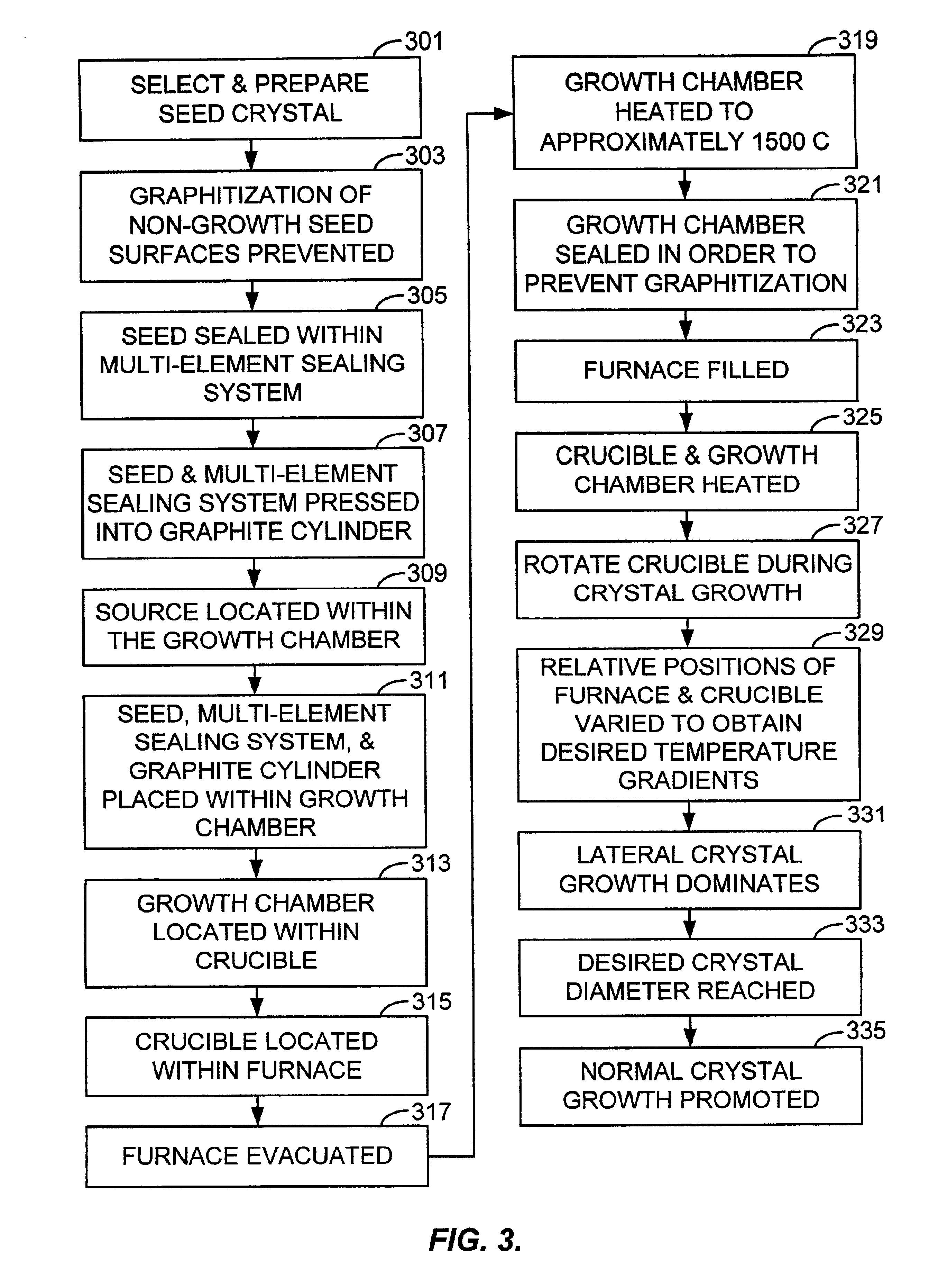
Embodiment Construction

a growth period of approximately 22 hours;

[0022]FIG. 10 illustrates a one dimensional temperature distribution over the ring element cell wall and the crystal interface;

[0023]FIG. 11 illustrates the ring element wall locations and the crystal interface locations that correspond to the data points shown in FIG. 10;

[0024]FIG. 12 illustrates the distribution of the principal component of the thermal elastic stress tensor as computed for the temperature distributions shown in FIG. 6; and

[0025]FIG. 13 illustrates the distribution of the principal component of the thermal elastic stress tensor as computed for the temperature distributions shown in FIG. 8.

DESCRIPTION OF THE SPECIFIC EMBODIMENTS

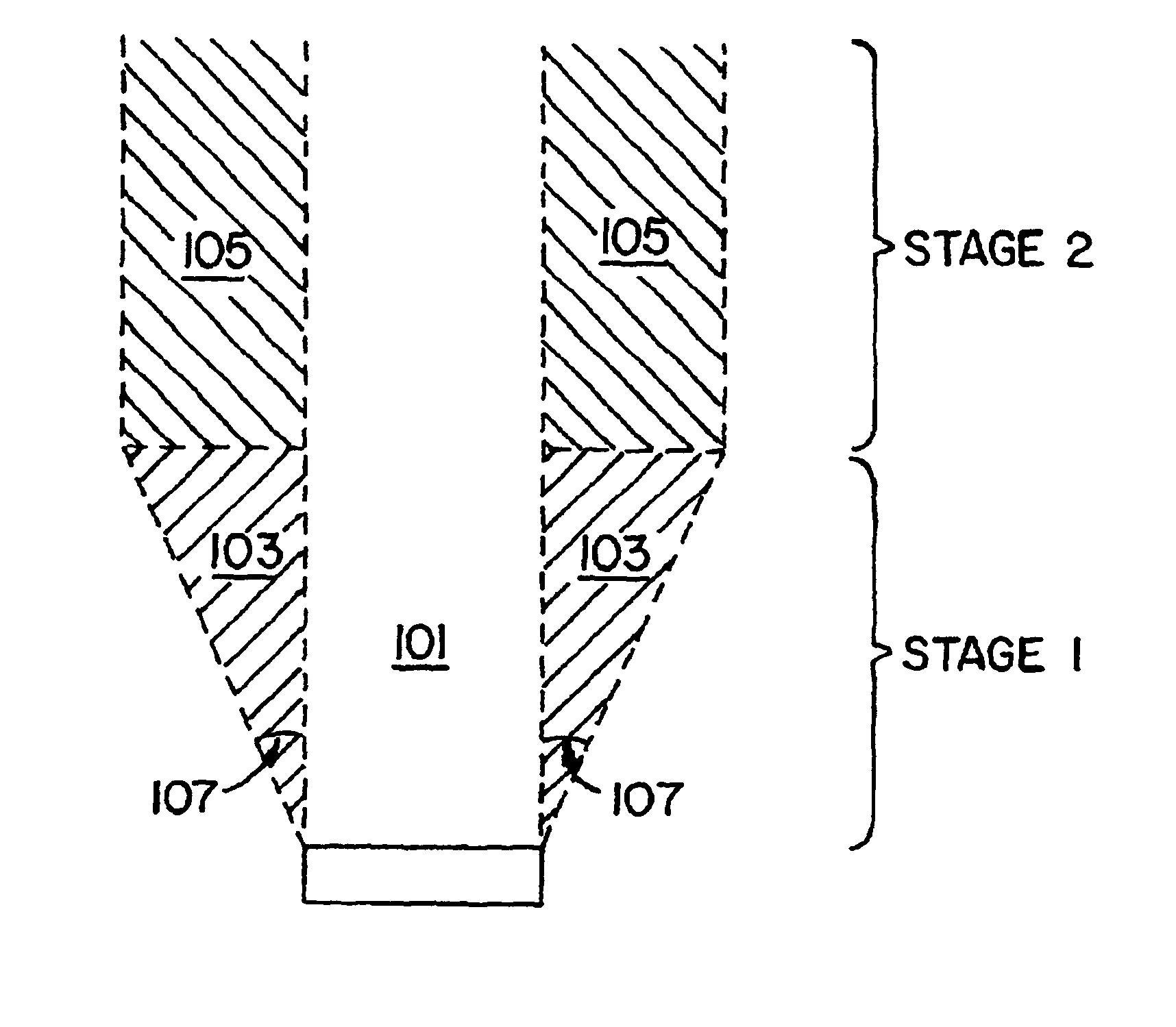
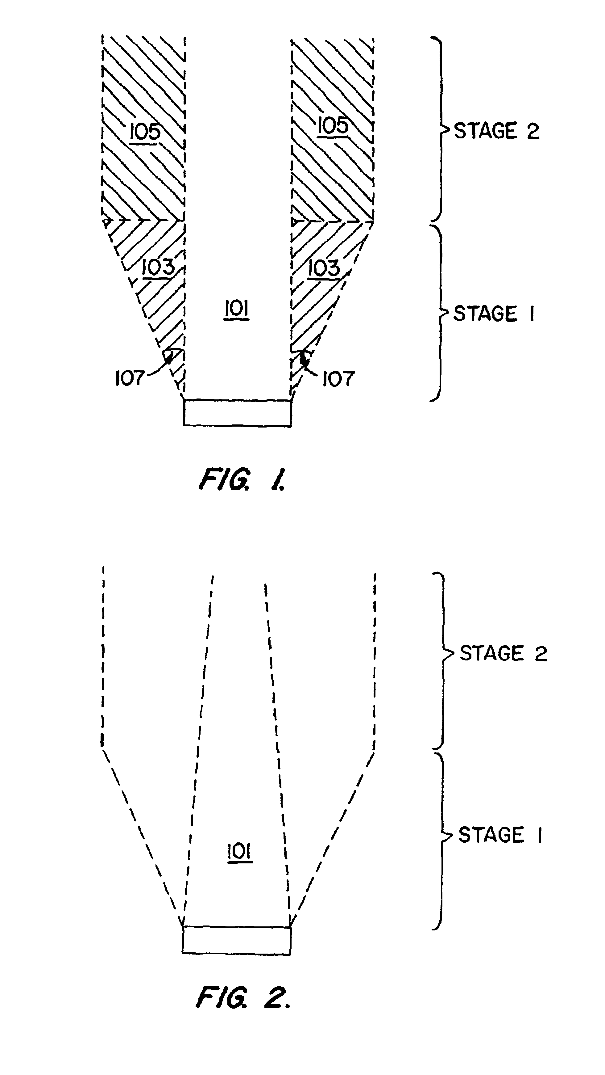
[0026]The dislocations in (0001) silicon carbide (SiC) seed crystals are primarily threading and screw dislocations in the crystal direction. Micropipe defects are basically screw dislocations with a Burger's vector that is so large that the core of the screw is empty. The inventors have found that ...


PUM


Abstract

A low defect (e.g., dislocation and micropipe) density silicon carbide (SiC) is provided as well as an apparatus and method for growing the same. The SiC crystal, grown using sublimation techniques, is preferably divided into two stages of growth. During the first stage of growth, the crystal grows in a normal direction while simultaneously expanding laterally. Although dislocations and other material defects may propagate within the axially grown material, defect propagation and generation in the laterally grown material are substantially reduced, if not altogether eliminated. After the crystal has expanded to the desired diameter, the second stage of growth begins in which lateral growth is suppressed and normal growth is enhanced. A substantially reduced defect density is maintained within the axially grown material that is based on the laterally grown first stage material.

Description

CROSS-REFERENCES TO RELATED APPLICATIONS[0002]This application is a continuation application of U.S. patent application Ser. No. 09 / 782,949, filed Feb. 14, 2001 now U.S. Pat. No. 6,508,880.FIELD OF THE INVENTION[0003]The present invention relates generally to silicon carbide and, more particularly, to a method and apparatus for growing low defect density silicon carbide.BACKGROUND OF THE INVENTION[0004]Silicon carbide (SiC) has a number of characteristics that make it an ideal candidate for a variety of semiconductor applications, primarily those requiring high power handling capabilities. Arguably the most important characteristic of SiC is its indirect bandgap, resulting in relatively high recombination lifetimes and the ability to produce higher voltage junctions than those that can be produced from a direct bandgap material. The large bandgap of this material also provides for negligible current leakage up to 500° C., thereby allowing for high temperature operation without exces...

Claims


Application Information

Patent Timeline
IPC IPC(8): C30B23/00
CPCC30B23/00C30B29/36Y10T117/10Y10S117/902Y10T117/1008
Inventor VODAKOV, YURY ALEXANDROVICHRAMM, MARK GRIGORIEVICHMOKHOV, EVGENY NIKOLAEVICHROENKOV, ALEXANDR DMITRIEVICHMAKAROV, YURY NIKOLAEVICHKARPOV, SERGEI YURIEVICHRAMM, MARK SPIRIDONOVICHHELAVA, HEIKKI I.
Owner THE FOX GROUP
Why Eureka
Try Eureka