Semiconductor production line multi-product workpiece combining method

A semiconductor and production line technology, applied in the fields of semiconductor/solid-state device manufacturing, electrical components, comprehensive factory control, etc., which can solve the problems of lack of systematic discussion and lack of research.

Inactive Publication Date: 2015-03-25
BEIJING UNIV OF CHEM TECH
View PDF6 Cites 6 Cited by
  • Summary
  • Abstract
  • Description
  • Claims
  • Application Information

AI Technical Summary

Problems solved by technology

The above methods either lack a systematic discussion of workpiece merging,

Method used


Image

  • Semiconductor production line multi-product workpiece combining method
  • Semiconductor production line multi-product workpiece combining method
  • Semiconductor production line multi-product workpiece combining method

Examples


Embodiment Construction

[0055] In order to better understand the technical solutions of the present invention, the implementation manners of the present invention will be further introduced below.

[0056] Take the semiconductor production scheduling standard model HP24 as an example for specific implementation. The model consists of 24 machining centers, with a total of 72 equipment, and the detailed parameters of some equipment are shown in Table 1.

[0057] Table 1 Some equipment parameters in the standard model HP24

[0058]

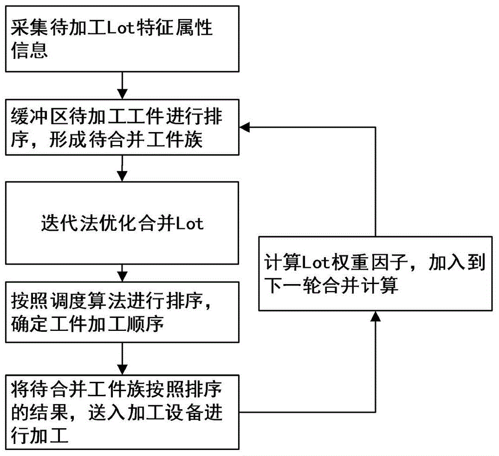
[0059] On the Plant Simulation simulation platform, the HP24 standard model is used for simulation. The dispatching rule adopts FIFO (First In First Out), the feeding strategy adopts CONWIP, the simulation time is set to 1445 hours, and the pre-simulation time is set to 365 hours. Figure 1-4 Shown is the main flowchart of the workpiece merging algorithm, including the following steps:

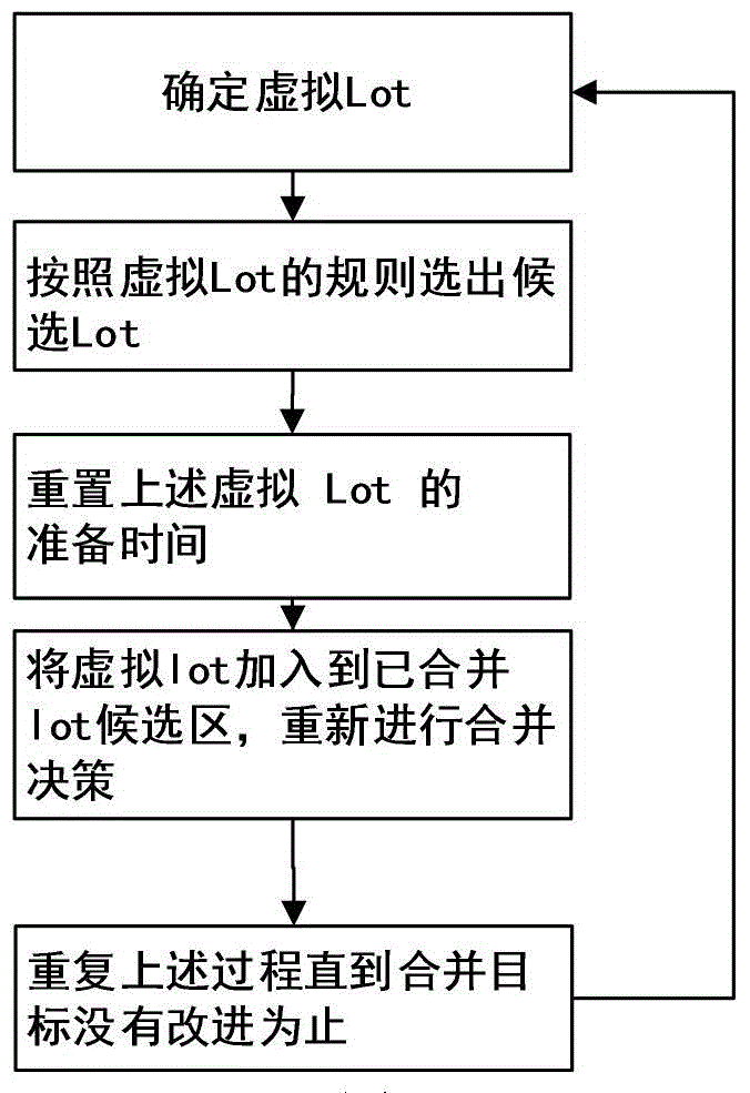
[0060] Step 1: Collect the Lot information to be processed in the buffer zone on t...


PUM


Abstract

Disclosed is a semiconductor production line multi-product workpiece combining method. The method comprises the steps that feature attributes of Lot to be machined in the processing equipment buffer area on a semiconductor production line are obtained; according to the collected workpiece feature attributes, on the basis of the semiconductor processing workpiece sorting compound rule, workpieces to be machined are sorted, and workpiece groups to be combined are formed; then, the ES/RW2 and MDBH combined scheduling algorithm is utilized for sorting the workpiece groups to be combined, and the workpiece processing sequence with the minimum tardiness as the optimization target is determined; finally, the workpiece groups to be combined are fed into processing equipment according to the sorting result to be machined, each Lot weighing factor of different order forms in the current round is calculated, and the technical support effect is provided for the combining decision for the next round. By optimizing the Lot processing flow of the same technology Lot of different order forms in the semiconductor production manufacturing process and combining the Lot processing time of the same technological menu, the production efficiency of the whole system will be improved, and the semiconductor production average processing period and order form tardiness rate are reduced.

Description

technical field [0001] The invention belongs to the technical field of semiconductor production scheduling and control, and relates to a method for merging workpieces of multiple products in a semiconductor production line. Background technique [0002] The semiconductor manufacturing industry is a high-tech industry with great strategic value for economic development. It has the characteristics of large-scale, high uncertainty, complex production process, complex constraints, and multi-objective. Under such circumstances, the maximization of production benefits and efficiency in the operation of semiconductor manufacturing enterprises has become an important issue to be solved urgently. Especially for large-scale integrated circuits and special-application integrated circuits, because of their large order volume and variety of products, it is necessary to optimize scheduling in the production process. [0003] At present, there are a large number of researches on semicondu...

Claims


Application Information

Patent Timeline
IPC IPC(8): G05B19/418H01L21/67
CPCG05B19/41865H01L21/67011Y02P90/02
Inventor 曹政才黄哲骁郝井华刘民
Owner BEIJING UNIV OF CHEM TECH
Why Eureka
Try Eureka