
Germanium etching method

A dry etching and germanium layer technology, applied in electrical components, semiconductor/solid-state device manufacturing, circuits, etc., can solve problems such as poor morphology and affect the performance of semiconductor devices, and achieve the effect of improving morphology and performance

Active Publication Date: 2015-03-25
SHANGHAI HUAHONG GRACE SEMICON MFG CORP
View PDF5 Cites 8 Cited by
  • Summary
  • Abstract
  • Description
  • Claims
  • Application Information

AI Technical Summary

Problems solved by technology

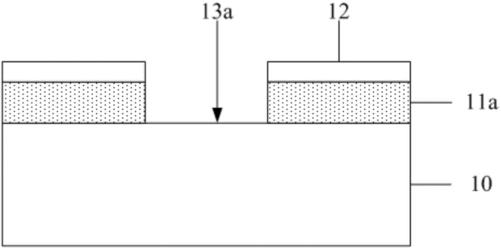
[0007] However, the patterned germanium layer 11a formed by the prior art has poor morphology, which affects the performance of the formed semiconductor device

Method used


Image

  • Germanium etching method
  • Germanium etching method
  • Germanium etching method

Examples


Embodiment Construction

[0028] It can be seen from the background technology that the morphology of the germanium layer formed by the existing germanium etching process is relatively poor. The reason is analyzed: the etching gas used in dry etching includes: chlorine gas (Cl 2 ), boron chloride (BCl 2 ), argon (Ar), nitrogen (N 2 ). Among them, chlorine gas is used as the main etching gas to react with the germanium layer to form germanium chloride (GeCl x ), the gas flow in the etched reaction chamber is taken out of the reaction chamber. However, when germanium is dry-etched, the germanium chloride generated by etching is easy to redeposit and adheres to the top or sidewall of the photoresist. The attached germanium chloride is difficult to remove by traditional etching methods. Moreover, the attached germanium chloride will affect the removal process of the photoresist, and the resulting germanium chloride is prone to redeposition, forming a germanium chloride polymer attached to the surface of...


PUM

PropertyMeasurementUnit
poweraaaaaaaaaa

Abstract

A germanium etching method comprises the steps that a semiconductor substrate is provided; a germanium layer is formed on the semiconductor substrate; part of the germanium layer is removed through a dry etching process, and gas in dry etching contains chlorine; after dry etching is performed, the etched germanium layer is washed with cleaning gas in situ, and the cleaning gas is oxygen. The germanium etching method can remove germanium chloride polymer adhering to the surface of photoresist in the etching process, the appearance of the etched germanium layer is improved, and the yield of formed semiconductor devices is improved.

Description

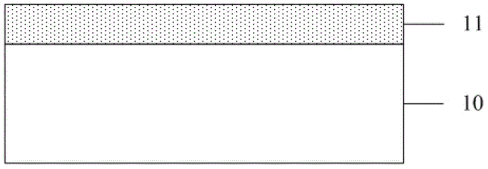
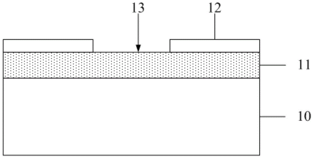
technical field [0001] The invention relates to the field of semiconductor manufacturing, in particular to a germanium etching method. Background technique [0002] Eutectic bonding, also known as eutectic bonding, refers to the technique of bonding wafers through a metallic interlayer. In the current field of semiconductor manufacturing, patterned germanium metal layers are widely used in eutectic bonding processes. [0003] To form a patterned germanium metal layer, germanium metal needs to be etched. For the process of etching germanium in the prior art, please refer to Figure 1 to Figure 3 ,include: [0004] refer to figure 1 , a semiconductor substrate 10 is provided, and a germanium layer 11 is formed on the surface of the semiconductor substrate 10 . [0005] refer to figure 2 , forming a patterned photoresist layer 12 on the surface of the germanium layer 11, the photoresist layer 12 has an opening 13 exposing part of the germanium layer 11, and the opening 13...

Claims


Application Information

Patent Timeline
Patent Type & Authority Applications(China)
IPC IPC(8): H01L21/3213
CPCH01L21/02071H01L21/32135
Inventor 熊磊奚裴
Owner SHANGHAI HUAHONG GRACE SEMICON MFG CORP
Learn More