Panel feeding and detecting device

A technology for inspection devices and panels, applied in the direction of electrical components, circuits, semiconductor/solid-state device testing/measurement, etc.

Inactive Publication Date: 2015-03-25
INTERFACE OPTOELECTRONICS SHENZHEN +1
View PDF6 Cites 3 Cited by
  • Summary
  • Abstract
  • Description
  • Claims
  • Application Information

AI Technical Summary

Problems solved by technology

[0005] The main purpose of the present invention is to provide a panel incoming inspection device, aiming to solve the technical problem of how to replace the manual visual inspection method

Method used


Image

  • Panel feeding and detecting device
  • Panel feeding and detecting device
  • Panel feeding and detecting device

Examples


Embodiment Construction

[0027] It should be understood that the specific embodiments described here are only used to explain the present invention, not to limit the present invention.

[0028] The invention is a panel feeding inspection device, which automates the panel picking and placing, improves the efficiency and accuracy of panel inspection, and at the same time reduces the risk of fragments caused by personnel during picking and placing operations.

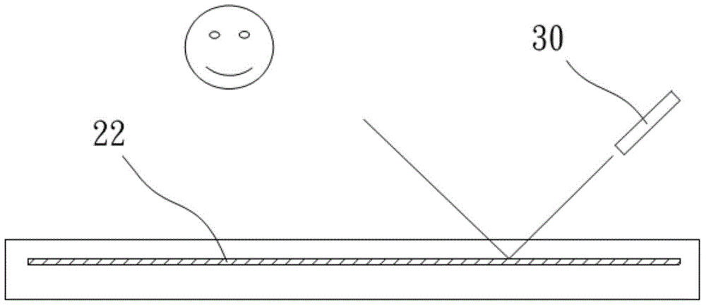
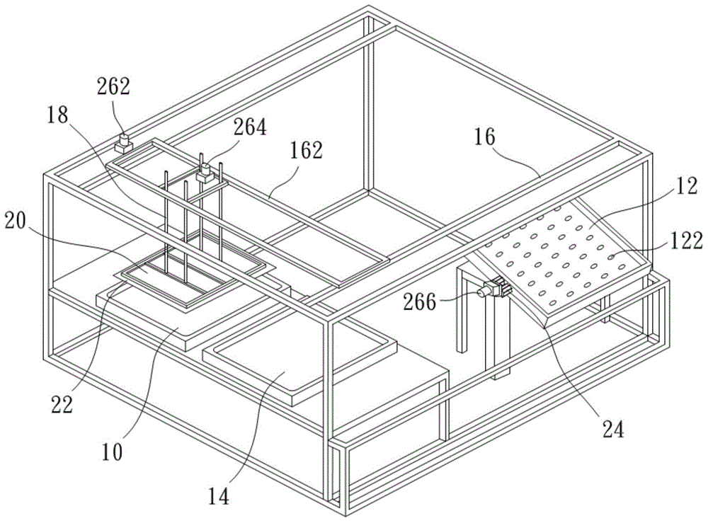
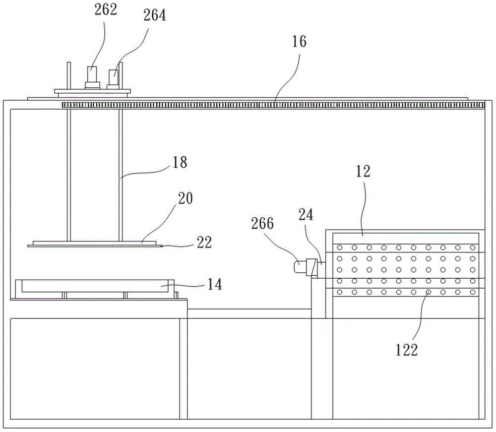
[0029] Please refer to figure 2 , which is a perspective view of the panel feeding inspection device of the present invention. The present invention includes a feeding place 10, a receiving place 14 and a light box 12, wherein the feeding place 10 is used to place the panel 22 to be inspected, and the light box 12 provides At least one light source 122, this light source 122 can be a light emitting diode (LED), when the panel 22 is placed on the light box 12, the light source 122 emits light and shines on the panel 22, and the reflected light of ...


PUM


Abstract

The invention discloses a panel feeding and detecting device which comprises a feeding position, a mechanical arm, a lamp box and a material collecting position. At least one panel is arranged at the feeding position, a sucker mechanism is arranged at the bottom of the mechanical arm, and the panel is sucked from the feeding position. The lamp box is provided with a light source illuminating panel, and the lamp box can overturn, and the mechanical arm moves to the lamp box so that the light source can illuminate the panel. The discharging position is used for carrying the detected panel. Thus, the process of feeding the panel, full automation of the process of detecting the panel and placing the panel to the discharging position can be achieved, manual carrying is not needed, the lamp box which can overturn by multiple angles is provided so that after the panel is placed on the lamp box, detecting in various angles can be conducted conveniently, the detecting efficiency and accuracy are improved, and the damage which may be caused by manual panel placing and taking is lowered.

Description

technical field [0001] The invention relates to a technology for inspection in the back-end process of wafers, in particular to a panel incoming inspection device. Background technique [0002] The Back-End-of-the-Line (BEOL) of the wafer is to place chips with the same optical and electrical characteristics on the same blue tape according to the electrical properties. Because they are arranged in a square shape, the output Also known as squares. During the production of the SBK section in the back-end process factory, some small pieces in the panel input material will be defective products. In order to control the defective input material, it is necessary to perform surface inspection on the panel input material before cutting. [0003] At present, the main inspection method is to inspect the surface of the chip with artificial vision and other light sources, such as figure 1 As shown, the panel 22 is irradiated with a hand-held flashlight 30 as a light source, and the vi...

Claims


Application Information

Patent Timeline
Patent Type & Authority Applications(China)
IPC IPC(8): H01L21/66
CPCH01L22/12
Inventor 蔡瑜于宗亚董宁袁斌
Owner INTERFACE OPTOELECTRONICS SHENZHEN
Why Eureka
Try Eureka