Flexible panel, method for manufacturing flexible panel and flexile display device

A flexible panel and flexible substrate technology, which is applied in the manufacture of electric solid devices, semiconductor devices, semiconductor/solid state devices, etc., can solve problems such as damage to flexible substrates, and achieve the effect of avoiding damage and ensuring performance

Inactive Publication Date: 2015-03-25
BOE TECH GRP CO LTD
View PDF4 Cites 11 Cited by
  • Summary
  • Abstract
  • Description
  • Claims
  • Application Information

AI Technical Summary

Problems solved by technology

[0005] In view of this, an embodiment of the present invention provides a flexible panel, its preparation method and a flexible display device, so as to prevent laser energy from being damaged due to the fact that the laser energy cannot be completely absorbed by the amorphous silicon film when forming a polysilicon film. flexible substrate

Method used


Image

  • Flexible panel, method for manufacturing flexible panel and flexile display device
  • Flexible panel, method for manufacturing flexible panel and flexile display device
  • Flexible panel, method for manufacturing flexible panel and flexile display device

Examples


preparation example Construction

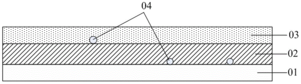
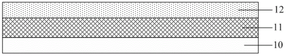
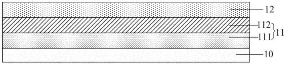
[0059] Based on the same inventive concept, the embodiment of the present invention also provides a method for preparing a flexible panel, such as Figure 4 As shown, the following steps may be included:

[0060] S101, forming a flexible substrate on a hard carrier substrate;

[0061] S102, forming a buffer layer on the flexible substrate, wherein the buffer layer has insulation and high thermal conductivity;

[0062] S103, forming an amorphous silicon thin film on the buffer layer;

[0063] S104 , performing laser crystallization treatment on the amorphous silicon film, so that the amorphous silicon film becomes a polysilicon film.

[0064] In the method for preparing the above-mentioned flexible panel provided by the embodiment of the present invention, before forming the amorphous silicon thin film, a buffer layer with insulation and high thermal conductivity is first formed on the flexible substrate. During the crystallization process, even if the laser energy cannot be...


PUM

PropertyMeasurementUnit
thicknessaaaaaaaaaa
thicknessaaaaaaaaaa
Overlap degreeaaaaaaaaaa

Abstract

The invention discloses a flexible panel, a method for manufacturing the flexible panel and a flexile display device. Due to the fact that a buffer layer is insulating and high in thermal conductivity, the insulating function is realized on one hand, and on the other hand, when laser crystallization is conducted on an amorphous silicon membrane on the buffer layer to form a polycrystalline silicon membrane, residual laser energy can still be dissipated quickly through the buffer layer high in thermal conductivity even if laser energy can not be absorbed totally by the amorphous silicon membrane. In this way, damage to a flexible substrate by the residual laser energy is avoided, and the performance of the flexible panel is guaranteed.

Description

technical field [0001] The invention relates to the technical field of semiconductors, in particular to a flexible panel, its preparation method and a flexible display device. Background technique [0002] Flexible display technology has been a research hotspot in the field of display technology in recent years. Because of its advantages of being thinner, more shock-resistant, and lighter, it will be widely used in civilian and military fields. Flexible display can be defined as the substrate of the display panel made of a very thin flexible substrate, which can be bent to a radius of curvature of only a few centimeters or less without damaging the display function of the display panel. [0003] At present, the active layer technology is the core technology of the display panel, and the low temperature polysilicon (Low Temperature Poly-Silicon, LTPS) thin film transistor (Thin Film Transistor, TFT) has a high electron mobility (up to >100cm2 / Vs) And stability, small size...

Claims


Application Information

Patent Timeline
Patent Type & Authority Applications(China)
IPC IPC(8): H01L27/12H01L21/02
Inventor 高涛毛雪杨静陈立强
Owner BOE TECH GRP CO LTD
Why Eureka
Try Eureka