Communication device

A communication device, Qualcomm's technology, which is applied to devices that make antennas work in different bands at the same time, the structure of radiation elements, electrical components, etc., and can solve problems such as low radiation efficiency.

Active Publication Date: 2015-03-25
ACER INC
View PDF5 Cites 12 Cited by
  • Summary
  • Abstract
  • Description
  • Claims
  • Application Information

AI Technical Summary

Problems solved by technology

This results in the inability to combine the resonant modes into a wide frequency band covering the required op

Method used


Image

  • Communication device
  • Communication device
  • Communication device

Examples


Embodiment Construction

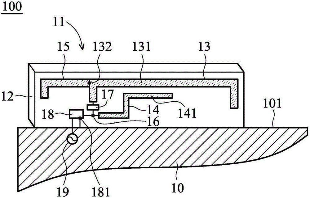
[0041] figure 1 is a schematic diagram showing the communication device 100 according to the first embodiment of the present invention. The communication device 100 can be a smart phone (Smart phone), a tablet computer (Tablet Computer), or a notebook computer (Notebook Computer). Such as figure 1As shown, the communication device 100 at least includes: a ground element 10 and an antenna element 11 . The ground element 10 can be a metal plane, which can be used to configure some electronic components (not shown) of the communication device 100 . The antenna element 11 may be made of metal. In some embodiments, the communication device 100 may further include: a dielectric substrate 12 , a first inductance element 17 , a high-pass matching circuit 18 , and a signal source 19 . The dielectric substrate 12 can be a FR4 (Flame Retardant 4) substrate. The first inductance element 17 can be a chip inductor (Chip Inductor). The high-pass matching circuit 18 may include one or m...


PUM


Abstract

A communication device comprises a grounding element and an antenna element. The antenna element has a first connection point, and at least comprises a first branch, a second branch and a third branch. One end of the first branch is coupled to the first connection point via an inductance element. One end of the second branch is coupled to the first connection point. A second section of the second branch is roughly parallel to a first section of the first branch. The second branch is arranged between the first branch and an edge of the grounding element. One end of the third branch is coupled to a second connection point on the first branch. The third branch and the first branch extend in roughly opposite directions. The first connection point is also coupled to a signal source via a high-pass matching circuit. A grounding end of the high-pass matching circuit is coupled to the grounding element. The antenna element of the communication device provided by the invention can be designed to be low in posture and small in size, and the antenna element can carry out operation in multiple bands including LTE/WWAN band and WLAN2.4GHz band.

Description

technical field [0001] The present invention relates to a communication device, in particular to a communication device including a small-sized multi-branch multi-band antenna element (Small-size Multi-branch Multi-band Antenna Element). Background technique [0002] Mobile communication technology is changing with each passing day, and its role in human life is getting heavier and heavier. Due to the different communication technologies in different eras and the different operating frequency bands of telecom operators in different regions, the demand for bandwidth of mobile communication devices is also increasing day by day. To facilitate portability and improve user experience, today's mobile communication devices tend to be thinner and lighter overall, and the size of their screens and frames will become smaller, and the space available for designing antennas will become less and less. Taking the traditional multi-branch multi-band LTE / WWAN (Long Term Evolution / Wireless...

Claims


Application Information

Patent Timeline
IPC IPC(8): H01Q1/38H01Q5/10H01Q5/20H01Q5/335H01Q5/371
Inventor 翁金辂林栢暐
Owner ACER INC
Why Eureka
Try Eureka