High Throw-Count RF Switch

a high throw-count, switch technology, applied in electronic switching, pulse technique, semiconductor devices, etc., can solve the problems of low rf performance, complicated design of such an ic, and the number of available transmit and/or receive paths, etc., to achieve good rf performance and high throw-count

Active Publication Date: 2017-08-10
PSEMI CORP
View PDF9 Cites 11 Cited by
  • Summary
  • Abstract
  • Description
  • Claims
  • Application Information

AI Technical Summary

Benefits of technology

[0008]The present invention encompasses a high throw-count multiple-pole FET-based RF switch architecture that provides good RF performance in terms of insertion loss, return loss, isolation, linearity, and power handling. In general, embodiments of the invention introduce additional common RF path branch isolation switches which are controlled by state dependent logic. The common RF path branch isolation switches can also be used to reconfigure the switch architecture for a multiplex function as well as separate switch path banks for re-configurability.
[0010]The added branch isolation switches are normally OFF (blocking), and only turned ON (conducting) when associated “far side” ports RFn are to be coupled to the common port RFC. The OFF state of each branch isolation switch helps to isolate the inactive branch ports RFn and the unused portion of the common path from the active, in-use portion of the common path. Thus, the branch isolation switches are used to effectively disconnect (i.e., isolate) inactive branches and thereby reduce the reactive load attributable to such branches that would otherwise degrade the RF performance of the ports RFn “closer” to the common port RFC. Reducing the reactive load on the common RF connection port significantly extends the operating bandwidth.
[0011]Embodiments of the invention provide good RF performance at high frequencies with switch throw-counts of more than 8 while exceeding the RF performance of conventional switch circuits with throw-counts of 8 or less at the same or lower frequencies.

Problems solved by technology

Moreover, in a multiple-pole FET-based RF switch IC, added impedance elements (e.g., inductors and / or transmission lines) as well as parasitic inductances caused by interconnections between FETs and by other circuit structures complicate the design of such an IC.
To date, such complications have limited the number of available transmit and / or receive paths in a multiple-pole FET-based RF switch to about 8 ports (plus a common port), and RF performance has been less than stellar.
In general, increasing the number of paths for an RF switch results in trade-offs with bandwidth and insertion loss (IL).
Additionally, adding throw counts creates extra parasitic inductances along signal paths which degrade performance due to asymmetry when different signal paths are active.
As another example, some 8 throw switches fabricated in GaAs have been created with useful bandwidths up to about 8 GHz, but at the expense of insertion loss, return loss quality, isolation, and linearity / power compression point.

Method used


Image

  • High Throw-Count RF Switch
  • High Throw-Count RF Switch
  • High Throw-Count RF Switch

Examples


first embodiment

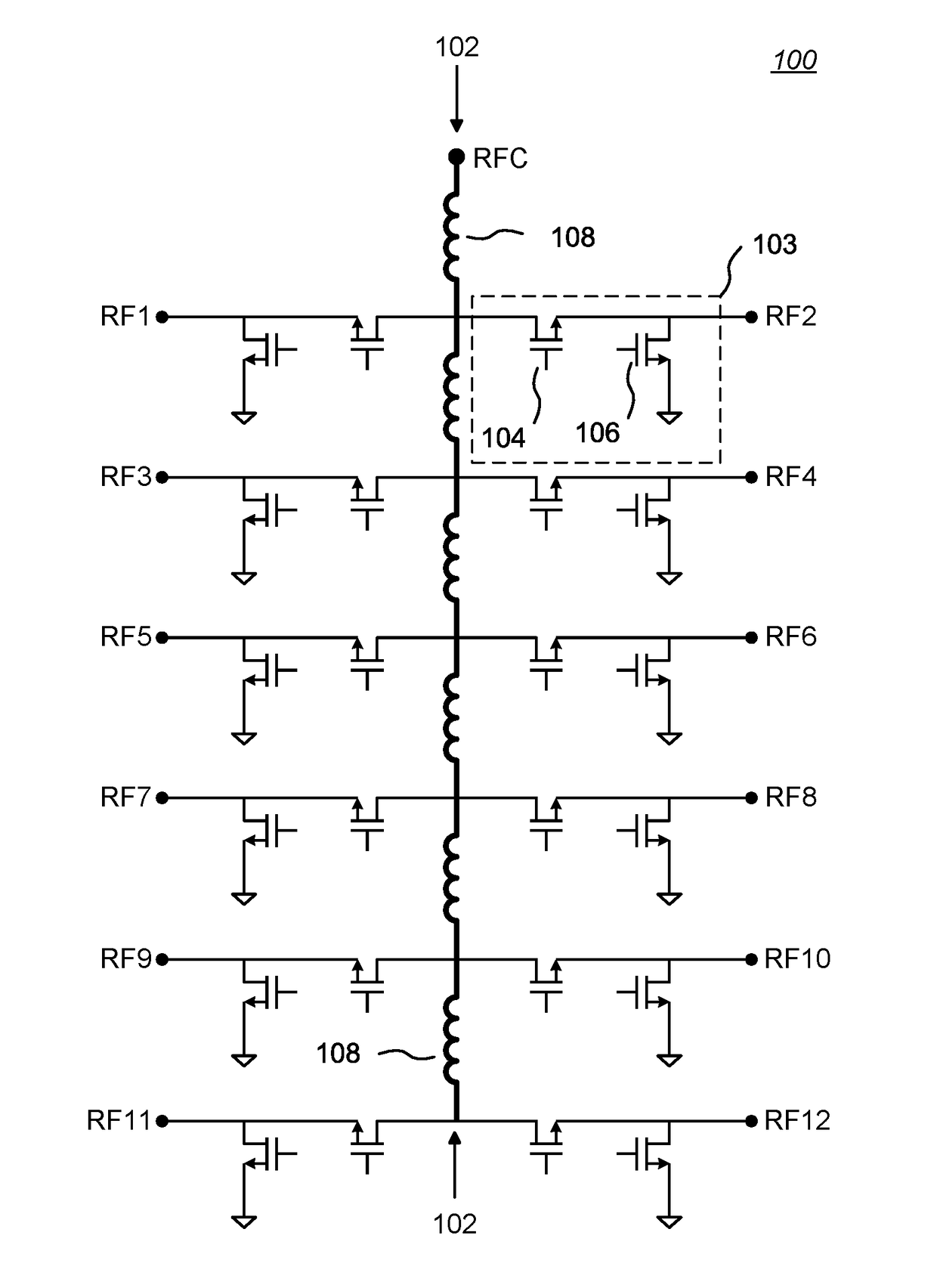
[0033]FIG. 3 is a schematic diagram of a first embodiment of a high throw-count RF switch 300 in conformance with the present invention. In the illustrated embodiment, the general switch architecture of FIG. 1 has been modified to include one or more branch isolation (BI) switches 302. Each BI switch 302 is independently switchable, the ON-OFF state of which depends on which port RFn is to be coupled to the common port RFC. In the illustrated example, two BI switches 302 (SW1 and SW2) define three sections A, B, C of branches. The control logic for the two BI switches 302 as a function of a single active port RFn would be as set forth in TABLE 2. Note that the RF1-RF12 designations may be assigned in any order; they are merely a label name for each port.

TABLE 2SectionActive PortBI Switch StateARF1-RF4SW1 = OFFSW2 = OFFBRF5-RF8SW1 = ONSW2 = OFFCRF9-RF12SW1 = ONSW2 = ON

[0034]Accordingly, the BI switches 302 are normally OFF (blocking), and only turned ON (conducting) when associated “...

second embodiment

[0041]FIG. 4 is a schematic diagram of a second embodiment of a high throw-count RF switch 400 in conformance with the present invention. The RFn ports are divided into two or more sub-divisions (two are shown, SD1, SD2), each having a common path 102a, 102b coupled to the common port RFC by a corresponding main branch isolation (BI) switch 402; two such switches SW1, SW2 are shown in the illustrated example. Within each sub-division SDn, further BI switches 404 may define separate sections or banks of ports RFn as in FIG. 3; one such switch (SW3, SW4) per sub-division SD1, SD2 is shown.

[0042]The illustrated configuration may be useful for certain package sizes (e.g., a 4×4 pad or pin package) and / or an application requirement calling for short IC bond wires to the RFn ports. The main BI switches 402 may help to bridge such distances and reduce IL for each signal path. Note that some optimization of FET switch widths for the series FETs of each port RFn may be necessary as well to c...

third embodiment

[0046]FIG. 5 is a schematic diagram of a third embodiment of a high throw-count RF switch 500 in conformance with the present invention. For compactness, the series-shunt switching elements 103 of FIG. 3 are shown as blocks labeled “S / S”, and the various inductors 108 of FIG. 3 are shown as blocks labeled “L”.

[0047]In the illustrated example, the common port RFC is positioned between the ends of the common path 102. The signal ports RFn (16 are shown by way of example) are coupled to the common path 102 so as to form multiple sub-groups (two are shown, G1, G2) of signal ports in a “butterfly” configuration (i.e., multiple banks Gn of signal ports arrayed around a centrally positioned common port RFC; thus, the concept is scalable). The common port RFC can be coupled to any of the ports RFn by activating appropriate ones of the intervening branch isolation switches SW1-SW4, similar to the operation of the architecture shown in FIG. 3. As in FIG. 3, in the illustrated embodiment, no p...


PUM


Abstract

A high throw-count multiple-pole FET-based RF switch architecture that provides good RF performance in terms of insertion loss, return loss, isolation, linearity, and power handling. A common port RFC is coupled along a common path to multiple ports RFn. Embodiments introduce additional common RF path branch isolation switches which are controlled by state dependent logic. The branch isolation switches help to isolate the unused branch ports RFn and the unused portion of the common path from the active portion of the common path, and thereby reduce the reactive load attributable to such branches that degrades RF performance of the ports RFn “closer” to the common port RFC. The branch isolation switches can also be used to reconfigure the switch architecture for a multiplex function as well as separate switch path banks for re-configurability of purpose, tuning, or varying switch throw counts and packaging options.

Description

BACKGROUND[0001](1) Technical Field[0002]This invention generally relates to electronic circuits, and more specifically to radio frequency (RF) switch circuits utilizing field effect transistors (FETs).[0003](2) Background[0004]Electronic signal switches are used in a wide variety of applications. In particular, a multiple-pole FET-based RF switch architecture has been found useful in applications which require multiple transmit and / or receive paths for RF signals. For example, such a switch architecture is useful in cellular radio systems for coupling multiple antennas to multiple sets of transmit / receive circuitry. Other examples include automatic test equipment and electronics laboratory bench measurement equipment.[0005]A FET may be fabricated in various technologies (e.g., standard bulk silicon, silicon-on-insulator, silicon-on-sapphire, GaN HEMT, GaAs pHEMT, and MESFET processes) and is commonly represented in schematic diagrams as an idealized ON-OFF switch device. However, i...

Claims


Application Information

Patent Timeline
Patent Type & Authority Applications(United States)
IPC IPC(8): H03K17/693H03K17/62H03K17/76
CPCH03K17/693H03K17/62H03K17/76H04B1/0458H04B1/48H03K2017/066H04B2001/485
Inventor SHAPIRO, ERIC S.SHANJANI, PAYMAN
Owner PSEMI CORP
Why Eureka
Try Eureka