Classification method of chip bin maps in wafer circuit probing

A technology of wafer testing and classification methods, which is applied in the direction of single semiconductor device testing, etc., can solve the problems of testing hardware damage, large leakage current, and long testing time, and achieve the effects of improving work efficiency, reducing quantity, and reducing testing time

Inactive Publication Date: 2015-04-01
SHANGHAI HUAHONG GRACE SEMICON MFG CORP
View PDF7 Cites 21 Cited by
  • Summary
  • Abstract
  • Description
  • Claims
  • Application Information

AI Technical Summary

Problems solved by technology

[0007] As can be seen from the above, the existing method will cause the test time to be relatively long due to the need to test the entire silicon chip, and the specific area needs to be divided into chips with designated FAIL BIN, that is, the FAIL BIN chips need to be classified; and for t

Method used


Image

  • Classification method of chip bin maps in wafer circuit probing
  • Classification method of chip bin maps in wafer circuit probing
  • Classification method of chip bin maps in wafer circuit probing

Examples


Embodiment Construction

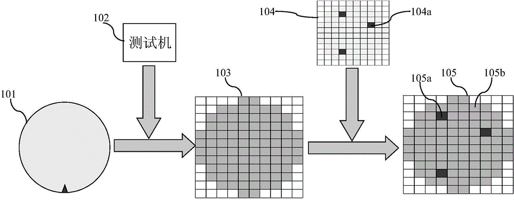
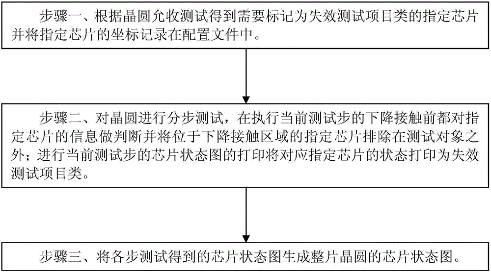
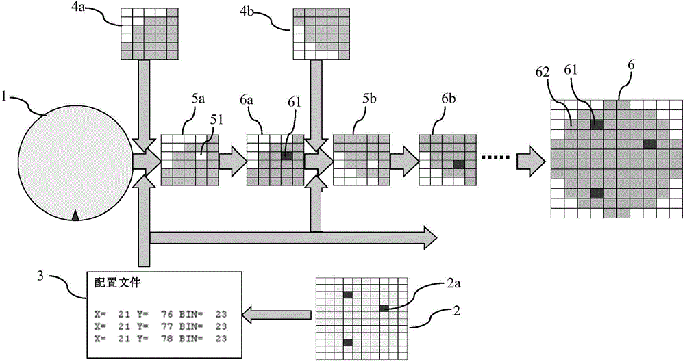
[0020] Such as figure 2 Shown is the flow chart of the classification method of the method wafer test chip state diagram of the embodiment of the present invention; image 3 As shown, it is a BIN MAP schematic diagram of the classification method of the wafer test chip state diagram according to the embodiment of the present invention. The classification method of wafer test chip state map in the embodiment of the present invention comprises the following steps:

[0021] Step 1. According to the results of the wafer acceptance test, it is judged that the chips in one or more specific areas of wafer 1 need to be changed to the failure test item category in the chip state diagram obtained from the wafer test, and will need to be marked as failure test items The chip of the class is defined as a specified chip and the coordinates of the specified chip are recorded in the configuration file 3 .

[0022] The coordinates of the specified chip recorded in the configuration file 3 ...


PUM


Abstract

The invention discloses a classification method of chip bin maps in wafer circuit probing. The method includes the steps that specified chips needing to be marked as fail bins are obtained according to a wafer acceptance test, and the coordinates of the specified chips are recorded in a configuration file; step-by-step testing is carried out on a wafer, information of all the specified chips is judged before touch down of the current test step is carried out, and specified chips located in a touch down area are excluded out of test objects; the chip bin map of the current test step is printed, and the state of the corresponding specified chip is printed as the fail bin; a chip bin map of the whole wafer is generated on the basis of the chip bin maps obtained in all the test steps. By means of the method, test time can be effectively shortened, test hardware can be effectively protected, a process flow can be simplified, error probability can be effectively reduced, and work efficiency can be effectively improved.

Description

technical field [0001] The invention relates to a semiconductor integrated circuit manufacturing process method, in particular to a classification method of wafer test chip state diagrams. Background technique [0002] Wafer testing (Circuit Probing, CP), also known as circuit needle testing, is to test the chip die (die) directly on the wafer (wafer) before packaging to verify whether each chip meets the product specifications. The CP test classifies the chips according to the test items (BIN) and forms a chip state map (BINMAP). The chips that fail the test need to be marked as failure test items (FAIL BIN) in the corresponding BINMAP. In the field of semiconductor integrated circuit manufacturing, a wafer refers to a single-crystal silicon wafer, referred to as a silicon wafer. For chips that fail the test, ink marks can also be directly placed on the wafer, so that chips marked as FAIL BIN in subsequent packages will be will not be selected. [0003] At present, custom...

Claims


Application Information

Patent Timeline
IPC IPC(8): G01R31/26
Inventor 朱渊源
Owner SHANGHAI HUAHONG GRACE SEMICON MFG CORP
Why Eureka
Try Eureka