Method for embedding at least one component into a printed circuit board

A technology for printed circuit boards and components, applied in the field of embedding at least one component in printed circuit boards, capable of solving problems such as device errors, adverse effects of contact connections, etc.

Active Publication Date: 2015-04-08
AT & S AUSTRIA TECH & SYSTTECHN AG
View PDF8 Cites 4 Cited by
  • Summary
  • Abstract
  • Description
  • Claims
  • Application Information

AI Technical Summary

Problems solved by technology

The devices used here lead to tolerances, especially when producing vias, which have a detrimental effect on the subsequently produ...

Method used


Image

  • Method for embedding at least one component into a printed circuit board
  • Method for embedding at least one component into a printed circuit board
  • Method for embedding at least one component into a printed circuit board

Examples


Embodiment Construction

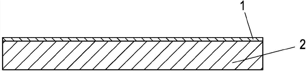
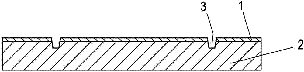
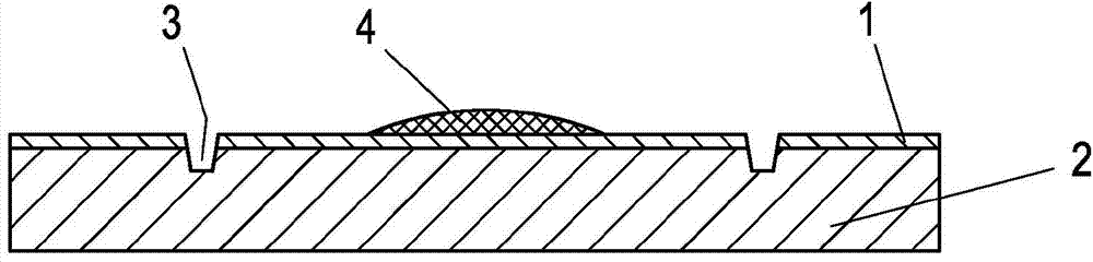
[0036] refer to Figures 1 to 10 , the method according to the invention for producing a printed circuit board comprising at least one embedded component, or such a printed circuit board according to the invention will be described as follows.

[0037] figure 1 The first step of the method is shown, specifically providing an underlying conductive thin foil 1, for example 2 micron copper foil, which is supported by a thicker underlying support layer 2, for example 70 micron copper foil, wherein layer 1 and 2 are connected to each other. The underlying conductive foil / support layer combination can also be provided with an insulating coating (not shown here), such as a resin layer, which is applied on the upper side, that is to say on the conductive foil 1, which is for example 5 to 15 microns thick . Due to such a coating, the relatively rough surface of the conductive foil (which usually consists of copper) is covered, which has proven to be expedient when fixing components ...


PUM


Abstract

The invention relates to a method for embedding at least one component into a printed circuit board, comprising the steps of providing a lower metallic conductor foil (1) applied on a first metallic supporting layer (2), forming recessed alignment marks (3) in the conductor foil (1), applying an adhesive layer (4) in a registered manner in relation to the alignment marks (3), and placing a component (5) with the rear side thereof on the adhesive layer (4) with connection areas (6) facing upwards, curing the adhesive layer, embedding the component (5) into an insulating layer (11), applying a metallic upper conductor foil (9) and an upper metallic supporting layer (10), consolidating the construction, removing the supporting layers (2, 10), exposing the alignment marks (3) of the lower conductor foil (1) by removing the insulating layer (11), producing cutouts (12) ending at the lower conductor foil (1), producing holes (13) to the connection areas (6) of the component (5) in a registered manner in relation to the alignment marks, and applying a conductor layer to the top side of the construction, producing contact-connections (14) in the holes (13) to the connection areas (6) of the component (5), and structuring the conductor layer for producing conductor tracks (15).

Description

technical field [0001] The invention relates to a method for embedding at least one component in a printed circuit board, said component being adhesively bonded to an underlying conductive foil with its connection area pointing upwards. [0002] The invention also relates to a printed circuit board comprising at least one embedded component, which is adhesively bonded to an underlying conductive foil and whose connection area points upwards, which is produced according to the method according to the invention. Background technique [0003] A component, such as a chip, can in principle be embedded in a printed circuit board "face-down" or "face-up". In the first case, the side of the component containing the contacts is connected to a metallic conductive layer, as shown for example in WO 2012 / 016258 A2 in the name of the applicant, while in the second case the opposite side of the component is connected to the The metallic conductive layer, that is to say on the side opposit...

Claims


Application Information

Patent Timeline
IPC IPC(8): H05K1/18H05K3/00
CPCH01L24/82H01L2224/82039H05K3/0008H05K1/188H01L2224/82132H01L2224/83132H01L2224/73267H01L2224/83129H01L24/24H01L2224/32245H01L2224/92244H01L2224/04105H01L2924/12042Y10T29/49133H01L2924/00H05K1/186H05K3/08H05K3/202H05K3/305
Inventor W·施里特魏泽尔
Owner AT & S AUSTRIA TECH & SYSTTECHN AG
Why Eureka
Try Eureka