Display panel, manufacturing method thereof and display device

A technology for display panels and array substrates, applied in nonlinear optics, instruments, optics, etc., can solve the problems of low integration and overall thickness of liquid crystal display devices

Active Publication Date: 2015-04-15
BOE TECH GRP CO LTD +1
View PDF7 Cites 7 Cited by
  • Summary
  • Abstract
  • Description
  • Claims
  • Application Information

AI Technical Summary

Problems solved by technology

[0005] Embodiments of the present invention provide a display panel, a manufacturing method thereof, and a display device to solve the proble

Method used


Image

  • Display panel, manufacturing method thereof and display device
  • Display panel, manufacturing method thereof and display device
  • Display panel, manufacturing method thereof and display device

Examples


Embodiment Construction

[0029] The specific implementation manners of the display panel provided by the embodiments of the present invention, its manufacturing method and the display device will be described in detail below with reference to the accompanying drawings.

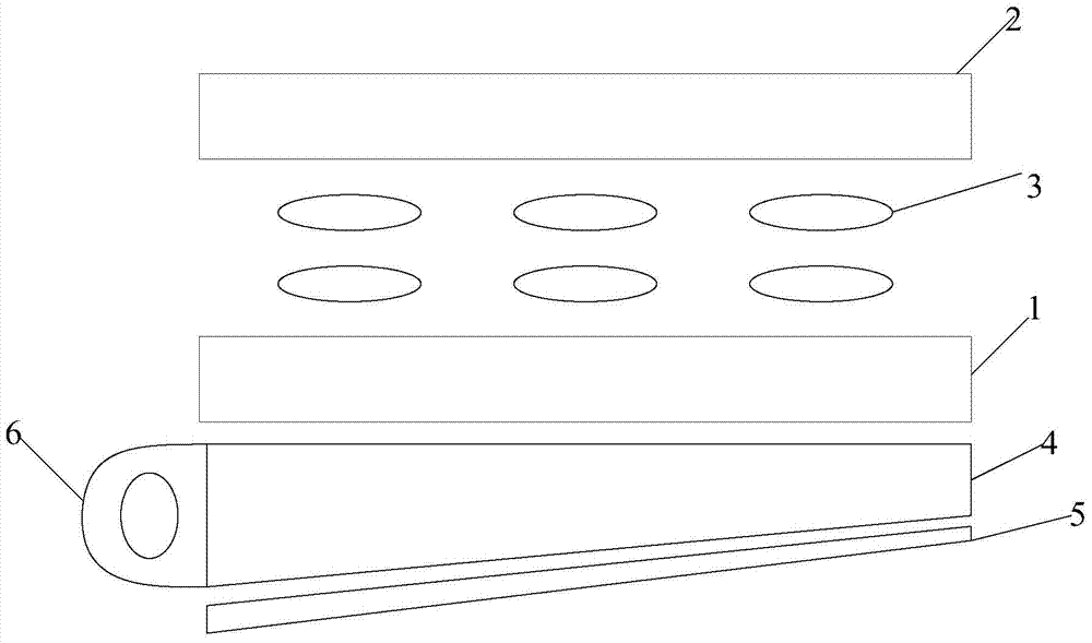
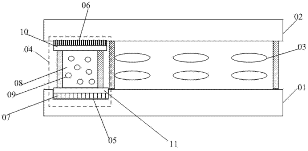
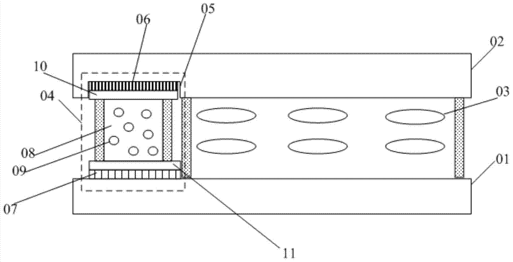
[0030] An embodiment of the present invention provides a display panel, such as Figure 2a-Figure 2c As shown, it may specifically include: an array substrate 01 and a counter substrate 03 facing each other, and a liquid crystal layer 03 encapsulated between the array substrate 01 and the counter substrate 02; and also includes:

[0031] at least one light emitting unit 04 packaged between the array substrate 01 and the opposite substrate 02 and located outside the liquid crystal layer 03;

[0032] The contact area between the base substrate of the array substrate 01 and / or the counter substrate 02 and the light emitting unit 04 has a groove structure 05 capable of accommodating the light emitting unit.

[0033] The above-mentioned d...


PUM

PropertyMeasurementUnit
Depthaaaaaaaaaa

Abstract

The invention discloses a display panel, a manufacturing method thereof and a display device. The display panel comprises an array substrate, an opposite substrate and a liquid crystal layer arranged between the array substrate and the opposite substrate, wherein at least one luminous unit is arranged between the array substrate and the opposite substrate, and is positioned on the outer side of the liquid crystal layer; (a) groove structure (s) for accommodating the luminous unit is/are formed in (a) contact areas of (a) backing substrate(s) of the array substrate and/or the opposite substrate and the luminous unit. According to the display panel, the manufacturing cost thereof and the display device, the distance between the array substrate and the opposite substrate is increased by the groove structures, so that an enough space for accommodating the luminous unit is formed between the array substrate and the opposite substrate; compared with the prior art with the problem of greater thickness of the whole display device caused by the thickness of a backlight source, the display panel has the advantages that the luminous unit is integrated between the array substrate and the opposite substrate through the groove structures, so that a backlight module can be thinned, the overall thickness of the display device can further be reduced, the integration level of the display device is improved, and the lightening and thinning development of the display device is facilitated.

Description

technical field [0001] The invention relates to the field of display technology, in particular to a display panel, a manufacturing method and a display device. Background technique [0002] At present, display technology is widely used in the display of televisions, mobile phones, and public information, and the flat-panel liquid crystal display used for displaying images has been vigorously promoted because of its ultra-thin and energy-saving advantages. [0003] Generally, the structure of a liquid crystal display device, such as figure 1 As shown, it mainly includes: a display panel composed of an array substrate 1, a color filter substrate 2, and a liquid crystal layer 3 located between the array substrate 1 and the color filter substrate 2, and a backlight module arranged under the display panel, wherein the backlight The module includes a light guide plate 4 set on the side of the array substrate 1 facing away from the liquid crystal layer 3 , a reflective plate 5 set...

Claims


Application Information

Patent Timeline
IPC IPC(8): G02F1/13357G02F1/1333G02F1/136
CPCG02F1/133603G02F1/133615G02F1/133614
Inventor 曲连杰郭建
Owner BOE TECH GRP CO LTD
Why Eureka
Try Eureka