Liquid crystal display panel

A technology for liquid crystal display panels and substrates, applied in nonlinear optics, instruments, optics, etc., can solve the problems of color shift of liquid crystal display panels, and achieve the effects of reducing color shift, improving display quality, and increasing spacing

Active Publication Date: 2015-04-22
XIAMEN TIANMA MICRO ELECTRONICS +1
View PDF6 Cites 7 Cited by
  • Summary
  • Abstract
  • Description
  • Claims
  • Application Information

AI Technical Summary

Problems solved by technology

[0003] In view of this, an embodiment of the present invention provides a liquid crystal display panel to solve the color shift problem of the liquid crystal display panel in the prior art

Method used


Image

  • Liquid crystal display panel
  • Liquid crystal display panel
  • Liquid crystal display panel

Examples


Embodiment 1

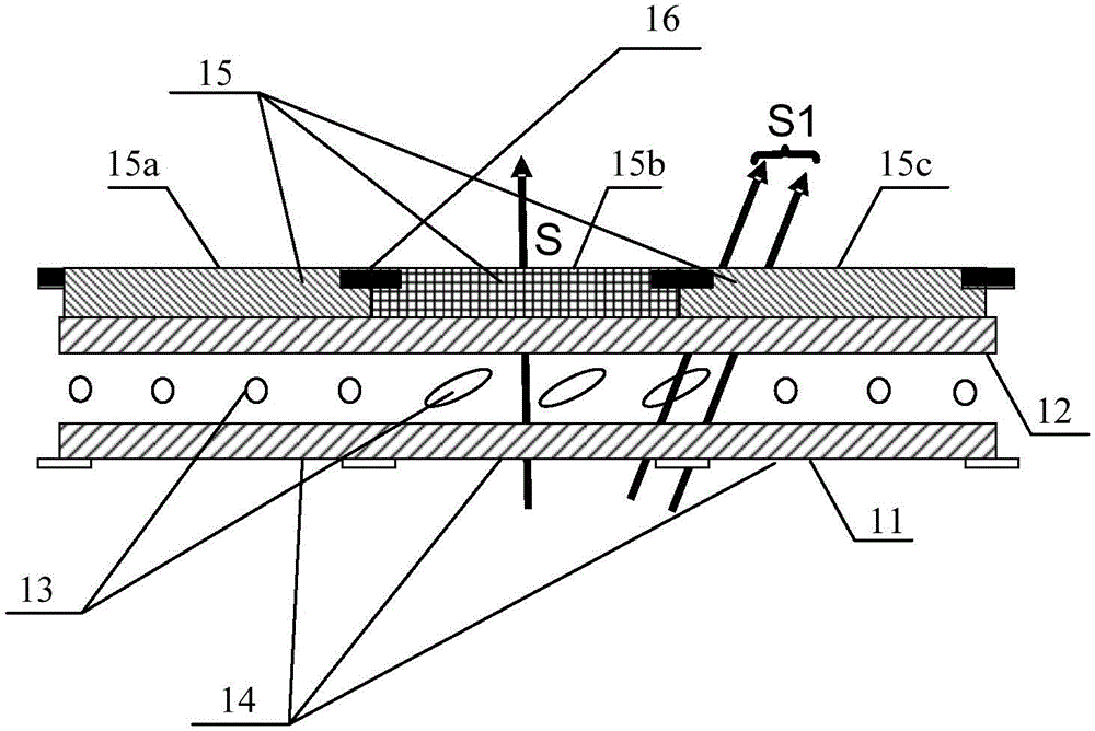
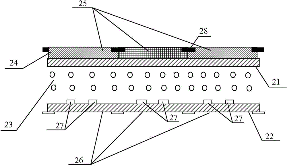
[0035] figure 2 It is a schematic structural diagram of a liquid crystal display panel in Embodiment 1 of the present invention. Such as figure 2 As shown, the liquid crystal display panel includes a first substrate 21 and a second substrate 22 oppositely arranged, and a negative liquid crystal 23 filled between the first substrate 21 and the second substrate 22; in addition, it also includes a color filter layer 24 , the color filter layer 24 includes at least two color resists 25 of different colors; the second substrate 22 includes at least two pixels 26 respectively corresponding to the at least two color resists 25, and each pixel 26 includes at least one sub- For the electrode 27, the width of the sub-electrode 27 on the pixel 26 corresponding to the color resistance with the largest transmittance is the largest.

[0036] Such as figure 2 As shown, the color filter layer 24 in Embodiment 1 of the present invention is arranged on the first substrate 21, but those sk...

Embodiment 2

[0043] In an embodiment of the present invention, each color resist on the color filter layer has multiple color matching modes, so as to realize the color display of the liquid crystal panel. In Embodiment 2 of the present invention, the technical scheme of displaying three primary colors on a liquid crystal display panel is mainly red, green, and blue. In this case, the color shift when displaying a red picture, that is, the color shift of red light serious.

[0044] Figure 4 It is a corresponding schematic diagram of the color filter layer and the pixel structure in Embodiment 2 of the present invention, as shown in Figure 4 As shown, the color filter layer 24 includes a red color resistance 251, a green color resistance 252 and a blue color resistance 253, and the second substrate 22 includes a first pixel 261 corresponding to the red color resistance 251, and a first pixel 261 corresponding to the green color resistance 252. The second pixel 262 is provided and the th...

Embodiment 3

[0050] In the third embodiment of the present invention, the description mainly focuses on the shape and size of each sub-electrode on each pixel.

[0051] Figure 7 It is a schematic illustration of the pixel structure in Embodiment 3 of the present invention Figure 1 ,Such as Figure 7 As shown, the first pixel 261 , the second pixel 262 and the third pixel 263 each include two parallel sub-electrodes 27 . Those skilled in the art can understand that, Figure 7 It is only an exemplary illustration, the above pixel may also include more parallel sub-electrodes 27 .

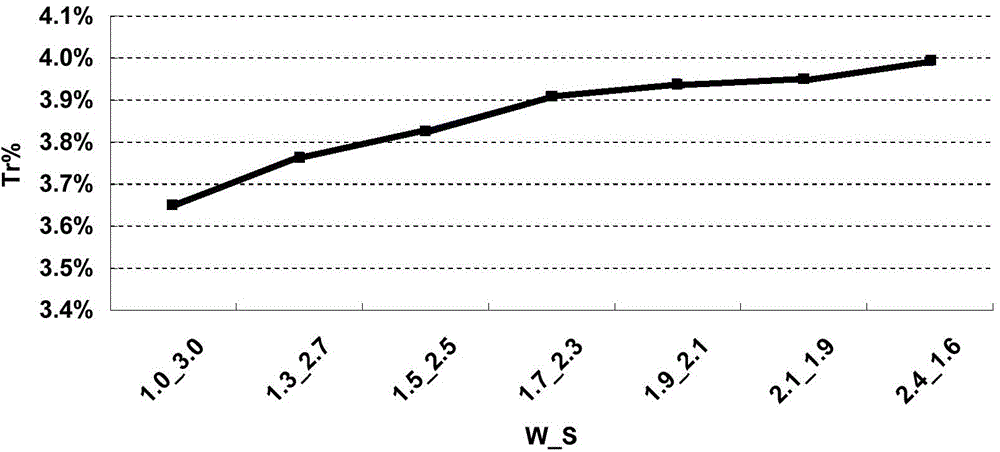
[0052] In addition, in Figure 7 Among them, the width of the sub-electrode 27 on the first pixel 261 is marked as W1, and the spacing between the sub-electrodes 27 on the first pixel 261 is marked as S1; the width of the sub-electrode 27 on the second pixel 262 is marked as W2, and The spacing between the sub-electrodes 27 on the second pixel 262 is marked as S2; the width of the sub-electrodes 27 on the t...


PUM

PropertyMeasurementUnit
widthaaaaaaaaaa

Abstract

The invention discloses a liquid crystal display panel. The liquid crystal display panel comprises a first substrate, a second substrate, negative liquid crystal and a color filter layer, wherein the first substrate and the second substrate are arranged oppositely, the space between the first substrate and the second substrate is filled with the negative liquid crystal, the color filter layer comprises at least two color resistors in different colors, the second substrate comprises at least two pixels corresponding to at least two color resistors respectively, each pixel comprises at least one sub-electrode, the sub-electrode on the pixel corresponding to the color resistor with the largest penetration rate has the maximum width, and the widths of the sub-electrodes on the pixels corresponding to the other resistors are smaller. By means of the liquid crystal display panel, the color cast phenomenon can be eliminated while the penetration rate of the liquid crystal display panel is effectively ensured.

Description

technical field [0001] The invention relates to the field of display technology, in particular to a liquid crystal display panel. Background technique [0002] Liquid crystal display is a display made of liquid crystal material, which has the characteristics of light and thin, low power consumption and large amount of displayed information. In liquid crystal display, the liquid crystal display panel is its most important component, figure 1 It is a structural schematic diagram of a liquid crystal display panel in the prior art, such as figure 1 As shown, a common liquid crystal display panel is mainly composed of an array substrate 11, a color filter substrate 12 arranged oppositely, and a liquid crystal layer 13 arranged between the array substrate 11 and the color filter substrate 12, and the array substrate 11 is arranged on the array substrate 11. A plurality of pixels 14; color-resistors 15 corresponding to each pixel are set on the color filter substrate 12. Generall...

Claims


Application Information

Patent Timeline
Patent Type & Authority Applications(China)
IPC IPC(8): G02F1/1335G02F1/1343
CPCG02F1/133514G02F1/134309G02F1/134345
Inventor 马扬昭
Owner XIAMEN TIANMA MICRO ELECTRONICS
Why Eureka
Try Eureka