

Method and device for clearing away information on complementary metal oxide semiconductor (CMOS)
A technology for clearing instructions and signals, applied in the field of clearing CMOS information, and can solve problems such as increased labor costs
- Summary
- Abstract
- Description
- Claims
- Application Information
AI Technical Summary
Problems solved by technology
Method used
Image

Examples
Embodiment Construction
[0049] The preferred embodiments of the present invention will be described in detail below in conjunction with the accompanying drawings. It should be understood that the preferred embodiments described below are only used to illustrate and explain the present invention, and are not intended to limit the present invention.
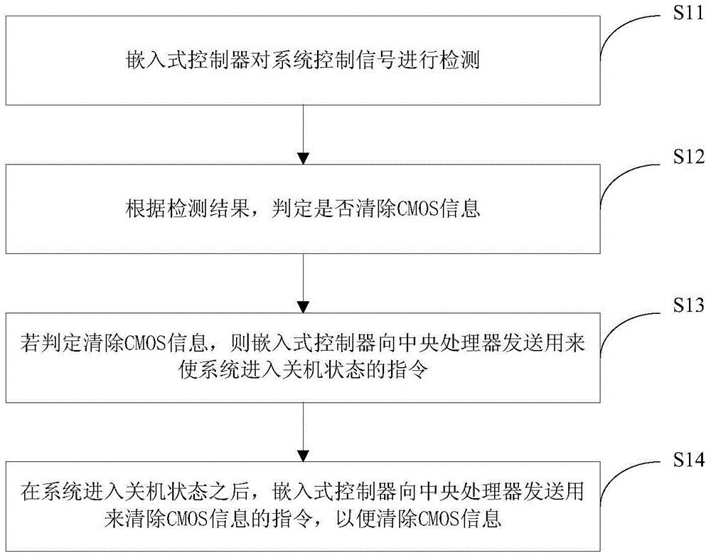
[0050] figure 1 It is a functional block diagram of the first method for clearing CMOS information provided by the embodiment of the present invention, such as figure 1 As shown, the steps include:
[0051] Step S11: The embedded controller detects the system control signal.
[0052] Step S12: According to the detection result, it is judged whether to clear the CMOS information.
[0053] Specifically, if the embedded controller detects the system control signal, it is judged whether the system control signal is a system control signal for clearing the CMOS information; Execute steps S13 and S14.
[0054] Step S13: If it is determined that the CMOS inf...
PUM
 Abstract
Description
Claims
Application Information