High-accuracy band gap reference voltage source

A technology of reference voltage source and reference voltage output, applied in the direction of adjusting electrical variables, control/regulating systems, instruments, etc.

Inactive Publication Date: 2015-04-29
CHANGSHA UNIVERSITY
View PDF5 Cites 10 Cited by
  • Summary
  • Abstract
  • Description
  • Claims
  • Application Information

AI Technical Summary

Problems solved by technology

[0004] In order to overcome the shortcomings that the temperature coefficient and power supply voltage rejection ratio of the existing traditional bandgap reference voltage source cannot meet the requirements of high-precision applications, the present invention proposes a high-precision bandgap quasi-voltage source, see the attached figure 1 , which is composed of a positive temperature coefficient generation circuit 1, a positive temperature coefficient compensation voltage generation circuit 2, and a reference voltage output circuit 3; it is composed of an operational amplifier OP, a first PMOS transistor PM1, a second PMOS transistor PM2, a third PMOS transistor PM3, The first NMOS transistor NM1, the first PNP transistor Q1, the second PNP transistor Q2, the first resistor R1, the second resistor R2, the power supply VCC, and the ground GND are connected to form a positive temperature coefficient current generation circuit 1; the fourth PMOS transistor PM4, the fifth PMOS transistor PM5, the second NMOS transistor NM2, the third NMOS transistor NM3, the third PNP transistor Q3, and the third resistor R3 are connected to form a positive temperature coefficient compensation current generating circuit 2; the sixth PMOS transistor PM6, the third The seven PMOS transistors PM7, the fourth NMOS transistor NM4, the fifth NMOS transistor NM5, the fourth PNP triode Q4, the fourth resistor R4, and the reference voltage output terminal Vref are connected to form a reference voltage output circuit; between the above three circuits The connections are: the power supply of the first PMOS transistor PM1 to the seventh PMOS transistor PM7 is connected to the power supply VCC; the gates of the third PMOS transistor PM3 to the seventh PMOS transistor PM7 are connected in common; the first PNP transistor Q1 to the third The bases and emitters of the four PNP transistors Q4 are connected in common; the drain of the fifth PMOS transistor PM5 in the positive temperature coefficient compensation current generating circuit is shared with the grid of the second NMOS transistor NM2 and the second resistor R2. The contact is connected to the gate of the fourth NMOS transistor NM4 in the output circuit 3 of the reference circuit

Method used


Image

  • High-accuracy band gap reference voltage source
  • High-accuracy band gap reference voltage source

Examples


specific Embodiment

[0008] Specific embodiments: the invention is further described as follows with reference to the accompanying drawings in conjunction with specific embodiments:

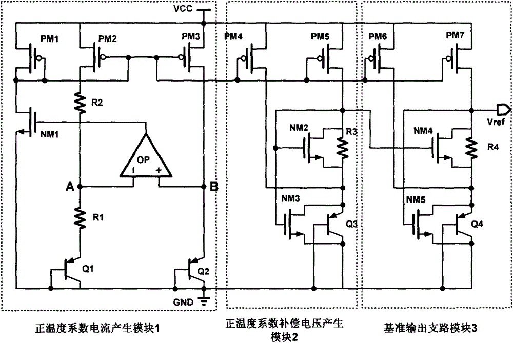
[0009] A high-precision bandgap reference voltage source circuit structure such as figure 1 As shown, it consists of the following parts: a positive temperature coefficient current generation circuit 1, a positive temperature coefficient compensation voltage generation circuit 2 and a reference output branch circuit 3.

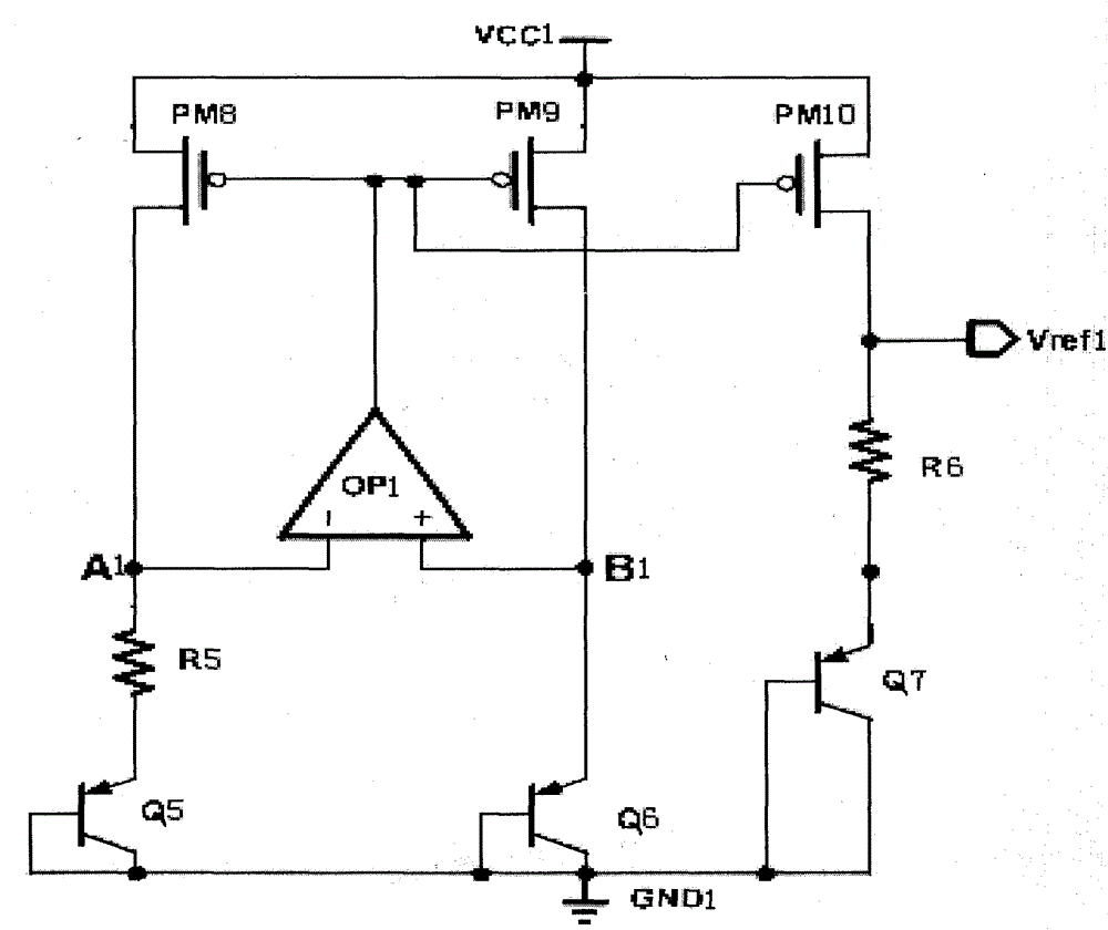
[0010] The positive temperature coefficient current generating circuit 1 is composed of an operational amplifier OP, a first PMOS transistor PM1, a second PMOS transistor PM2, a first NMOS transistor NM1, a first PNP transistor Q1, a second PNP transistor Q2, a first resistor R1, and a second resistor R2 is connected; the base stages of the first PNP transistor Q1 and the second PNP transistor Q2 are both grounded and connected in a diode manner. The operational amplifier makes the potentials of A a...


PUM


Abstract

The invention relates to a high-accuracy band gap reference voltage source. The high-accuracy band gap reference voltage source is formed by connecting an operational amplifier OP, a plurality of PMOS transistors PM, a plurality of NMOS transistors NM, a plurality of PNP triodes Q and a plurality of resistors R; a method of respectively carrying out temperature compensation in positive and negative temperature intervals is adopted to respectively shunt a current by the NMOS tubes on the resistors and the triodes so as to fulfill the aim; by introducing a negative feedback between the operational amplifier OP and a power supply VCC, a voltage rejection ratio of the band gap reference voltage source is improved, so that the band gap reference voltage source obtains a high-accuracy reference voltage; the high-accuracy band gap reference voltage source has a temperature coefficient of 8.20 ppm/DEG C and below within a temperature range from minus 40 to 120 DEG C, has a power supply voltage rejection ratio of 83.0dB under the low frequency and can be widely applied to a civil or military integrated circuit required to be supplied with a high-accuracy reference potential.

Description

Technical field: [0001] The invention belongs to the field of bandgap reference voltage sources in integrated circuits. Background technique: [0002] The bandgap reference voltage source is one of the important components of many chips. It has many applications where high-precision reference potentials are required, such as comparators, ADCs, and DACs. Its performance has a great impact on chip performance. The main indicators to measure the performance of the bandgap reference voltage source are the temperature coefficient and the power supply voltage rejection ratio. With the development of technology and more stringent applications, the high-precision performance indicators of the bandgap reference voltage source are getting higher and higher. [0003] The circuit structure of the existing traditional bandgap reference voltage source is as follows: figure 2 As shown, it mostly adopts the first-order temperature compensation method, which is composed of the eighth PMOS t...

Claims


Application Information

Patent Timeline
Patent Type & Authority Applications(China)
IPC IPC(8): G05F1/56
Inventor 李正大
Owner CHANGSHA UNIVERSITY
Why Eureka
Try Eureka