Shifting register and driving method thereof

A shift register, shift register circuit technology, applied in static memory, digital memory information, instruments, etc., can solve the problems of abnormal display of display units, abnormal drive of display units, etc., to ensure the effect of normal driving

Active Publication Date: 2015-04-29
SHANGHAI TIANMA MICRO ELECTRONICS CO LTD +1
View PDF8 Cites 33 Cited by
  • Summary
  • Abstract
  • Description
  • Claims
  • Application Information

AI Technical Summary

Problems solved by technology

[0005] The embodiment of the present invention provides a shift register and its driving method, which is used to solve the problem that the thin-film transistors in the gate driving device in the prior art will cause abnormality in the driving of the display unit due to the drift of the threshold voltage, resulting in the failure of the display unit. abnormal display problem

Method used


Image

  • Shifting register and driving method thereof
  • Shifting register and driving method thereof
  • Shifting register and driving method thereof

Examples


Embodiment 1

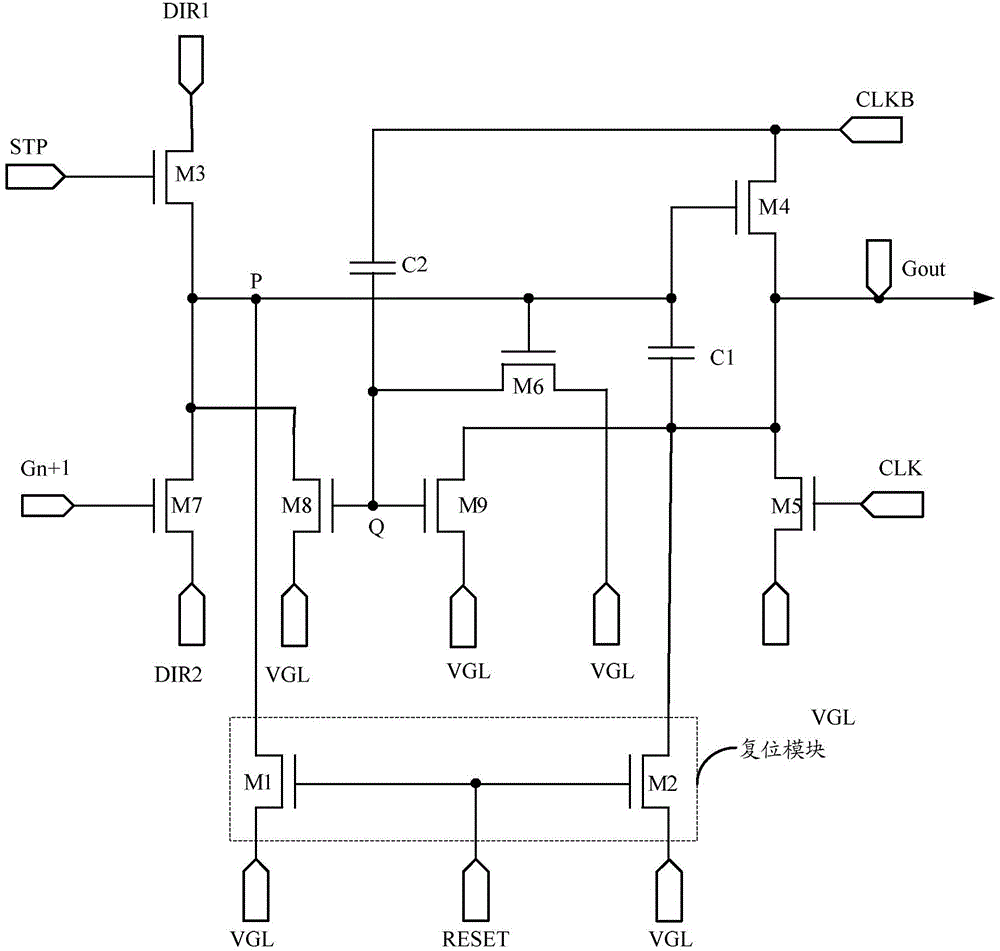
[0048] Such as figure 1 A circuit diagram of a shift register circuit is shown, which includes 9 thin film transistors, 2 capacitors C1 and C2, wherein the reset module includes two thin film transistors M1 and M2, and a switch thin film transistor M3, which is used to output the drive signal Thin film transistors M4 and M5, thin film transistors M6, M7, M8, M9 for pull-down potential. Among them, the first node is P, the second node is Q, Gout is the main output, the main input terminal STP is used to input the initial signal, Gn+1 is the input terminal of the signal fed back from the output terminal of the next-level shift register circuit, VGL It is a low-level signal source, an input terminal of the reset signal Reset, an input terminal of the first clock signal CLK, and an input terminal of the second clock signal CLKB, wherein the first clock signal CLK and the second clock signal CLKB are inverted. Such as figure 1 The driving process of the shift register circuit to ...

Embodiment 2

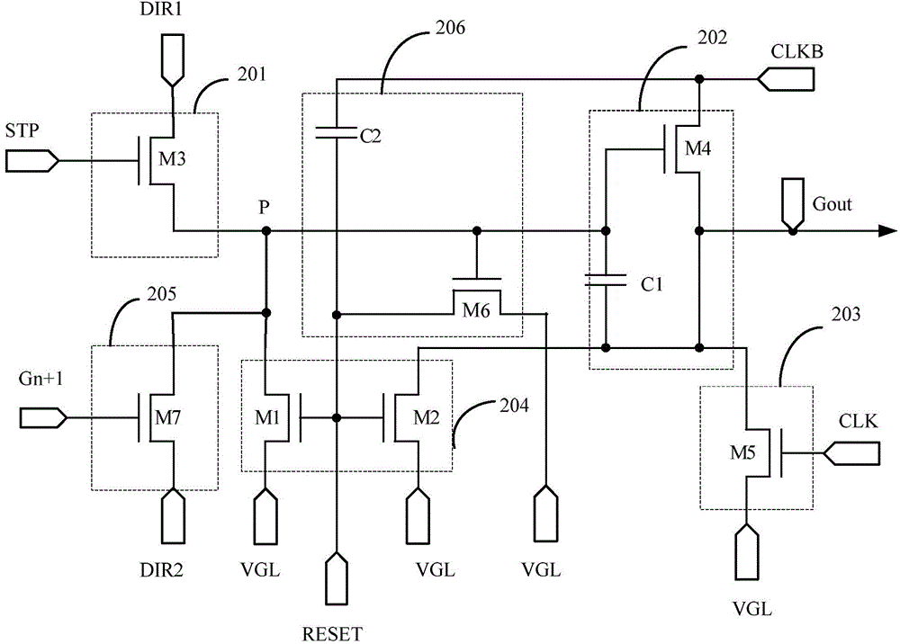
[0058] Such as figure 2 The shown embodiment of the present invention provides a shift register, the shift register includes a multi-stage cascaded shift register circuit, and each stage of the shift register circuit includes:

[0059] The main output terminal Gout is used to output drive signals, including high-level drive signals and low-level drive signals;

[0060] a main input module 201, configured to receive an initial signal STP;

[0061] The first output module 202 is connected between the main input module 201 and the main output terminal Gout, and is used to output a high-level driving signal according to the second clock signal. The main input module 201 and the first output The node between the modules 202 is the first node P;

[0062] The second output module 203 is connected to the main output terminal Gout, and is used to output a low-level driving signal according to the first clock signal;

[0063] It also includes: a first reset module 204, configured to...

Embodiment 3

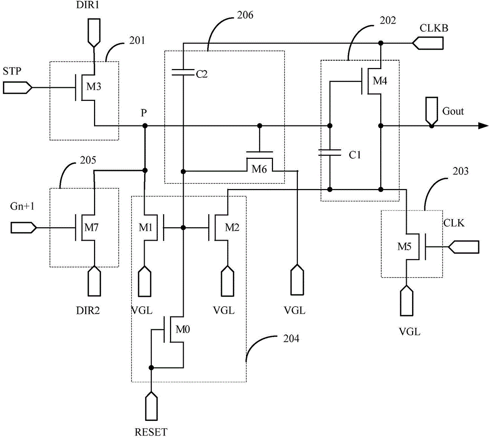
[0073] Such as image 3 A kind of shift register provided by an embodiment of the present invention is shown, the shift register includes multi-stage cascaded shift register circuits, and each stage of shift register circuits is figure 2 On the basis of the shift register circuit shown, a thin film transistor M0 is added in the first reset module, such as image 3 As shown, the shift register circuit includes: a main output terminal Gout for outputting driving signals, including high-level driving signals and low-level driving signals;

[0074] a main input module 201, configured to receive an initial signal STP;

[0075] The first output module 202 is connected between the main input module 201 and the main output terminal Gout, and is used to output a high-level driving signal according to the second clock signal. The main input module 201 and the first output The node between the modules 202 is the first node P;

[0076] The second output module 203 is connected to the ...


PUM


Abstract

The invention discloses a shifting register and a driving method thereof. The shifting register comprises a plurality stages of cascaded shifting register circuits, a first reset module and a second reset module, wherein each stage of shifting register circuit comprises a main output end, a main input module, a first output module and a second output module; the node between each main input module and each first output module is a first node; the first reset module is used for resetting the first nodes and the main output ends to low level according to a first reset signal input by a reset signal input end; the second reset module is used for receiving a second reset signal output by the next stage of shifting register circuit to reset the first nodes and the main output ends to low level. Before inputting an initial signal, the first reset module resets voltage of the first nodes and the main output ends, so that the gate driving signals are not influenced by the threshold voltage shifting of thin film transistors and the problem that the display units display abnormally due to the threshold voltage shifting of the thin film transistors in the prior art is solved.

Description

technical field [0001] The invention relates to the technical field of liquid crystal flat panel display, in particular to a shift register and a driving method thereof. Background technique [0002] A liquid crystal display (LCD) generally consists of a liquid crystal display panel and an external driving device, which is used to provide a driving signal for a display unit. At present, the driving device integrated on the display panel can make the structure of the display more compact, for example, the amorphous silicon gate driving device integrated on the display panel provides the gate driving signal for the pixel unit of the display panel, because Thin film transistor technology is relatively mature, with good uniformity and low cost, so amorphous silicon gate driving devices are widely used in liquid crystal displays. [0003] The shift register in the amorphous silicon driving device includes a plurality of shift register units, and the shift register circuit of eac...

Claims


Application Information

Patent Timeline
Patent Type & Authority Applications(China)
IPC IPC(8): G09G3/36G11C19/28
Inventor 孙云刚
Owner SHANGHAI TIANMA MICRO ELECTRONICS CO LTD
Why Eureka
Try Eureka