Preparation method of power diode

A power diode, N-type technology, applied in semiconductor/solid-state device manufacturing, electrical components, circuits, etc., can solve problems such as high reverse leakage current, short reverse recovery time, and large forward voltage drop of PN junction diodes

Active Publication Date: 2017-08-08
CSMC TECH FAB2 CO LTD
View PDF6 Cites 0 Cited by
  • Summary
  • Abstract
  • Description
  • Claims
  • Application Information

AI Technical Summary

Problems solved by technology

However, a PN junction diode has a large forward voltage drop and a long reverse recovery time; a Schottky diode has a small forward voltage drop and a short reverse recovery time, but its reverse leakage current is relatively high

Method used


Image

  • Preparation method of power diode
  • Preparation method of power diode
  • Preparation method of power diode

Examples


Embodiment Construction

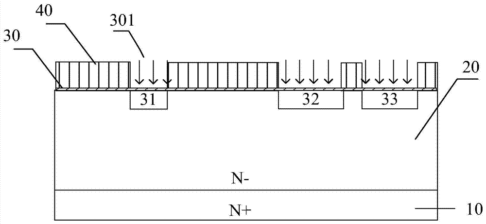
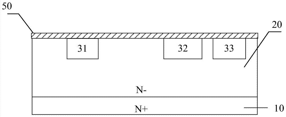
[0018] In order to make the objects, features and advantages of the present invention more comprehensible, specific implementations of the present invention will be described in detail below in conjunction with the accompanying drawings. In this specification and drawings, reference signs N and P assigned to layers or regions indicate that these layers or regions include a large number of electrons or holes, respectively. Further, the reference marks + and − assigned to N or P indicate that the concentration of the dopant is higher or lower than in layers not so assigned to the marks. In the description of the embodiments below and the drawings, similar components are assigned similar reference numerals and redundant descriptions thereof are omitted here.

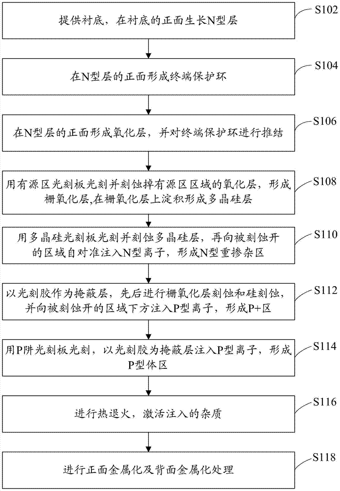
[0019] Such as figure 1 Shown is a flow chart of a method for preparing a power diode according to an embodiment. The preparation method includes the following steps.

[0020] S102, providing a substrate, and growing an ...


PUM


Abstract

The invention provides a preparation method of a power diode. The preparation method comprises the following steps: providing a substrate and growing an N type layer on the substrate; forming a terminal protection ring; forming an oxide layer, and performing knot guiding on the terminal protection ring; using a photoetching plate to photoetch in an active region, and etching off the oxide layer in the active region area, after removing of the photoresist, forming a gate oxide layer on the front of the N type layer in the active region area, and depositing a polycrystalline silicon layer on the gate oxide layer; forming an N type heavily doped region; forming a P+ region; using a P trap photoretching plate to perform photoetching, injecting P type ion by taking the photoresist as a masking layer to form a P type body region; performing thermal annealing to activate the injected impurities; performing front metallization and back metallization. According to the preparation method of the power diode, the N type heavily doped region and the P+ zone of the device are firstly prepared, and then the P type body region is prepared, so that the feature size of the P trap photoetching plate can be adjusted to adjust the length of an MOS channel, and the relation between the reverse leakage current and the forward voltage drop of the device can be optimized.

Description

technical field [0001] The invention relates to the technical field of semiconductor manufacturing, in particular to a method for preparing a power diode. Background technique [0002] Diode is a rapidly developing and widely used power electronic device. Diodes can be divided into rectifier diodes, detector diodes, and limiter diodes according to their uses. Traditional rectifier diodes mainly include PN junction diodes and Schottky diodes. However, the PN junction diode has a large forward voltage drop and a long reverse recovery time; the Schottky diode has a small forward voltage drop and a short reverse recovery time, but its reverse leakage current is relatively high. Contents of the invention [0003] Based on this, it is necessary to provide a preparation method that can optimize the relationship between the reverse leakage current and the forward voltage drop of the power diode to address the above problems. [0004] A method for preparing a power diode, compri...

Claims


Application Information

Patent Timeline
Patent Type & Authority Patents(China)
IPC IPC(8): H01L21/329
CPCH01L29/6609
Inventor 邓小社钟圣荣王根毅周东飞张大成
Owner CSMC TECH FAB2 CO LTD
Why Eureka
Try Eureka