A method for preparing a composite mask for high-energy ion implantation

A composite mask and high-energy ion technology, which is applied in semiconductor/solid-state device manufacturing, electrical components, circuits, etc., can solve the problems of easy residual photoresist mask, many process errors of pattern size, and poor film adhesion. Achieve the effect of avoiding device process failure, avoiding mask residue, and completely removing the mask

Active Publication Date: 2017-08-15
SHANGHAI INST OF TECHNICAL PHYSICS - CHINESE ACAD OF SCI
View PDF2 Cites 0 Cited by
  • Summary
  • Abstract
  • Description
  • Claims
  • Application Information

AI Technical Summary

Problems solved by technology

Although the hard mask avoids the bombardment denaturation and residual problems of the photoresist mask, it needs to deposit an additional dielectric film, and perform multi-step photolithography and etching, and the process is complex
The reasons why the hard mask is not suitable for HgCdTe devices are: 1) The deposition temperature of the hard mask layer is far beyond the temperature range (below 70°C) that the HgCdTe material can withstand, while the low temperature growth (2 , graphite, amorphous carbon, etc.) have a large lattice mismatch with HgCdTe materials, and the adhesion of the film is poor; 3) the hard mask requires multi-step photolithography and pattern etching, and the introduced pattern size There are many process errors, which makes it difficult to guarantee the pattern accuracy of the small-size implantation area

Method used


Image

  • A method for preparing a composite mask for high-energy ion implantation
  • A method for preparing a composite mask for high-energy ion implantation
  • A method for preparing a composite mask for high-energy ion implantation

Examples


Embodiment 1

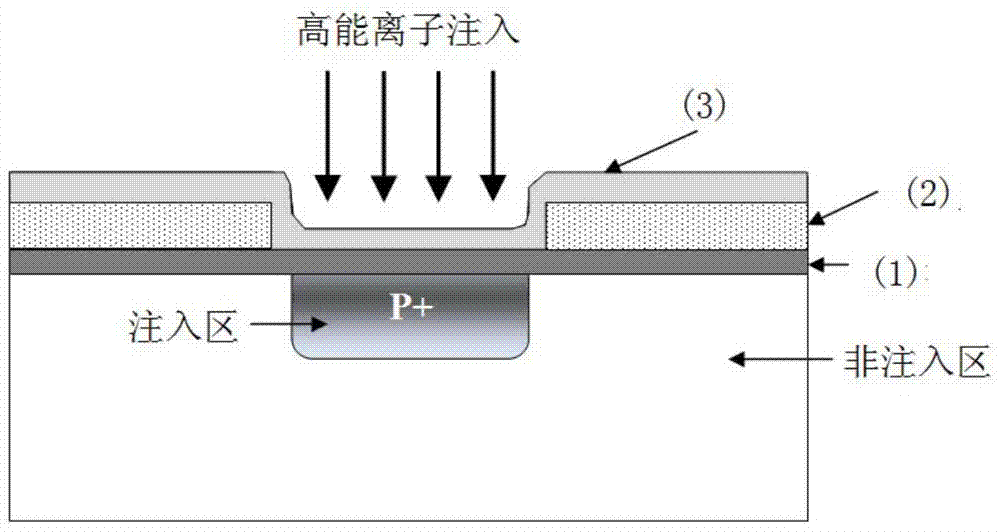
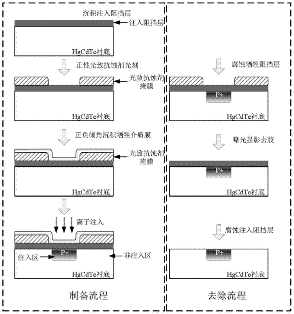
[0025] Using the mask preparation method described in the present invention, evaporation deposition, photolithography, and positive and negative inclination angle evaporation deposition are carried out on the surface of the mercury cadmium telluride epitaxial material chip. The preparation process is shown in the attached figure 2 shown. Firstly, a cadmium telluride injection barrier layer with a thickness of ~60nm is deposited by thermal evaporation on the surface of the HgCdTe epitaxial material chip after annealing treatment and surface corrosion treatment, the chip is cleaned, and a layer of 2-3 microns in thickness is spin-coated on the chip surface A thick positive photoresist is used to expose the chip to ultraviolet light with a photolithography plate, and after developing and fixing, a photoresist injection mask is obtained.

[0026] Load the chip with the mask pattern prepared on the sample stage of the high-vacuum thermal evaporation equipment, first rotate the sam...

Embodiment 2

[0030] Using the mask preparation method described in the present invention, evaporation deposition, photolithography, and positive and negative inclination angle sputter deposition are carried out on the surface of the mercury cadmium telluride epitaxial material chip. The preparation process is shown in the attached figure 2shown. First, thermally evaporate and deposit ~20nm thick cadmium telluride implant barrier layer on the surface of the HgCdTe epitaxial material chip after annealing treatment and surface corrosion treatment, clean the chip, and spin coat a layer of 2-3 microns in thickness on the chip surface A thick positive photoresist is used to expose the chip to ultraviolet light with a photolithography plate, and after developing and fixing, a photoresist injection mask is obtained.

[0031] Load the chip with the prepared mask pattern on the sample stage of the magnetron sputtering equipment, first rotate the sample stage at an inclination angle of 0°, and sputt...

Embodiment 3

[0035] Using the mask preparation method described in the present invention, evaporation deposition, photolithography, and positive and negative inclination angle evaporation deposition are carried out on the surface of the mercury cadmium telluride epitaxial material chip. The preparation process is shown in the attached figure 2 shown. First, thermally evaporate and deposit ~200nm thick cadmium telluride implant barrier layer on the surface of the HgCdTe epitaxial material chip after annealing treatment and surface corrosion treatment, clean the chip, and spin coat a layer of 2-3 microns in thickness on the chip surface A thick positive photoresist is used to expose the chip to ultraviolet light with a photolithography plate, and after developing and fixing, a photoresist injection mask is obtained.

[0036] Load the chip with the mask pattern prepared on the sample stage of the high-vacuum thermal evaporation equipment, first rotate the sample stage at an inclination angle...


PUM


Abstract

The invention discloses a preparation method of a composite mask for high-energy ion implantation. The mask is a composite photoresist mask with a three-layer structure, a photoresist mask figure of the composite mask is made between an implantation barrier layer dielectric film and a surface layer sacrifice dielectric film, and is used for high-energy ion implantation of the mask. The preparation method comprises the steps that the mask figure is formed on the surface of the implantation barrier layer dielectric film through positive photoresist in a photoetching mode, and the surface layer sacrifice dielectric film grows in an injection region, and the side wall and the top end of the photoresist mask through a positive and negative inclination film evaporation technology, and is used for high-energy ion implantation. The composite mask can solve the problem that the photoresist mask chaps and denatures under the high-energy ion bombardment, no residue is left when the mask is removed, the surface cleanliness of a chip is guaranteed, and device performance is improved.

Description

technical field [0001] The invention relates to mask technology in microelectronic technology, in particular to a method for preparing a composite mask used for HgCdTe high-energy ion implantation. Background technique [0002] Infrared focal plane array detectors based on mercury cadmium telluride photodiodes have been widely used in military security, resource exploration, ocean monitoring, and space remote sensing. According to the device structure, HgCdTe photodiodes can be divided into n-on-p type and p-on-n type. The n-on-p process has matured after decades of technology accumulation, and the short-wave infrared (SWIR) and mid-wave infrared (MWIR) HgCdTe FPA devices based on this process have already had high performance. However, for long-wave (LW) and very long-wave (VLW) devices, in order to obtain the spectral response of the corresponding band, the band gap of the HgCdTe base material must be further reduced (<90meV). In such a narrow bandgap, the tunneling c...

Claims


Application Information

Patent Timeline
Patent Type & Authority Patents(China)
IPC IPC(8): H01L21/266
CPCH01L21/266
Inventor 施长治林春
Owner SHANGHAI INST OF TECHNICAL PHYSICS - CHINESE ACAD OF SCI
Why Eureka
Try Eureka