A detachable fpga verification development board with high-speed operation

A development board, high-speed technology, applied in the field of verification development board, can solve the problems of FPGA chip damage, high price, troublesome replacement of FPGA chip, etc., to meet the needs of design verification and convenient disassembly and assembly

Active Publication Date: 2017-11-10
SHANDONG HUAYI MICRO ELECTRONICS
View PDF9 Cites 0 Cited by
  • Summary
  • Abstract
  • Description
  • Claims
  • Application Information

AI Technical Summary

Problems solved by technology

Usually, the FPGA chip is directly soldered on the development board, or the FPGA chip is soldered on the PCB adapter board, and then connected to the development board through the adapter board. There is a problem: when the FPGA chip is damaged or the capacity and speed of the FPGA cannot To meet the demand, when it needs to be replaced, it will be very troublesome to replace the FPGA chip, requiring professional equipment, and the expensive FPGA chip may be damaged during the operation

Method used


Image

  • A detachable fpga verification development board with high-speed operation
  • A detachable fpga verification development board with high-speed operation

Examples


Embodiment Construction

[0014] The present invention will be further described and defined below in conjunction with the accompanying drawings and specific embodiments.

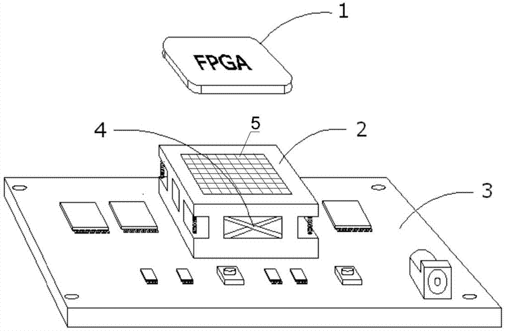
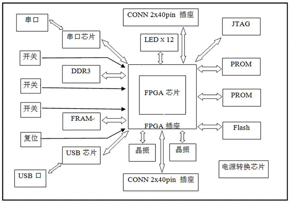
[0015] Such as figure 1 Shown, a kind of FPGA detachable and the verification development board of high-speed operation, comprise development board 3, be positioned at the socket 2 on the development board 3 and detachably be connected on the FPGA chip 1 on the socket 2, development board 3 is provided with and The pad corresponding to the packaging form of the socket 2, the socket 2 is soldered on the pad; the socket 2 is provided with a pin 5 corresponding to the solder ball of the FPGA chip 1, and the upper end of the pin 5 is connected to the solder ball of the FPGA chip 1 The lower end is connected to the wiring on the development board 3, and the FPGA chip 1 is electrically connected to each component on the development board 3 through the pin 5 of the socket 2.

[0016] In this embodiment, the FPGA chip 1 is detachably conne...


PUM


Abstract

The invention discloses a detachable and high-speed verification development board for FPGA, comprising a development board, a socket located on the development board and an FPGA chip detachably connected to the socket. The socket is welded on the pad; the socket is provided with a pin corresponding to the FPGA solder ball, the upper end of the pin is connected to the solder ball of the FPGA chip, and the lower end is connected to the trace on the development board. The chip is electrically connected to the components on the development board through the pins of the socket; in order to cooperate with the fast running speed of the FPGA chip, a memory that can access data at a high speed (Flash chip, FRAM chip and DDR3 chip) is arranged around it. ), according to FPGA programming, these chips can be called individually or simultaneously to ensure the high-speed operation of the development board. The FPGA chip can be disassembled and assembled manually on the development board, no other equipment is required, the disassembly and assembly is convenient, and the chip will not be damaged, and can be disassembled and assembled repeatedly; at the same time, the design of the development board gives full play to the advantages of the FPGA chip in parallel processing of data. Can fully meet the needs of design verification.

Description

technical field [0001] The invention relates to an FPGA-based verification and development board, in particular to a verification and development board with detachable FPGA and high-speed operation, belonging to the field of computer hardware. Background technique [0002] The verification development board based on FPGA (Field Programmable Gate Array, Field Programmable Gate Array) is a circuit board developed to meet the needs of design verification by utilizing the advantages of FPGA chip field programmable and data parallel processing. High-speed FPGA chip. Usually, the FPGA chip is directly soldered on the development board, or the FPGA chip is soldered on the PCB adapter board, and then connected to the development board through the adapter board. There is a problem: when the FPGA chip is damaged or the capacity and speed of the FPGA cannot To meet the demand, when it needs to be replaced, it will be very troublesome to replace the FPGA chip, requiring professional eq...

Claims


Application Information

Patent Timeline
Patent Type & Authority Patents(China)
IPC IPC(8): G09B23/18G05B19/042
CPCG09B23/186
Inventor 王磊王明宇邓波
Owner SHANDONG HUAYI MICRO ELECTRONICS
Why Eureka
Try Eureka