Supercharge Your Innovation With Domain-Expert AI Agents!

Graph production method, array substrate and display device

A manufacturing method and graphics technology, applied in semiconductor/solid-state device manufacturing, optics, instruments, etc., can solve the problems of light leakage at the edge of the pixel area, chaotic arrangement of liquid crystal molecules, and inability to refract light in the expected direction, so as to avoid light leakage and improve friction The effect of craft

Active Publication Date: 2015-05-13
BOE TECH GRP CO LTD +1
View PDF2 Cites 2 Cited by
  • Summary
  • Abstract
  • Description
  • Claims
  • Application Information

AI Technical Summary

Problems solved by technology

In this way, the PI film in the blind area is not rubbed and the liquid crystal molecules are disordered, so that the light cannot be refracted in the expected direction, and light leakage at the edge of the pixel area occurs.

Method used


Image

  • Graph production method, array substrate and display device
  • Graph production method, array substrate and display device
  • Graph production method, array substrate and display device

Examples


Embodiment Construction

[0028] In order to make the technical problems, technical solutions and advantages to be solved by the present invention clearer, the following will describe in detail with reference to the drawings and specific embodiments.

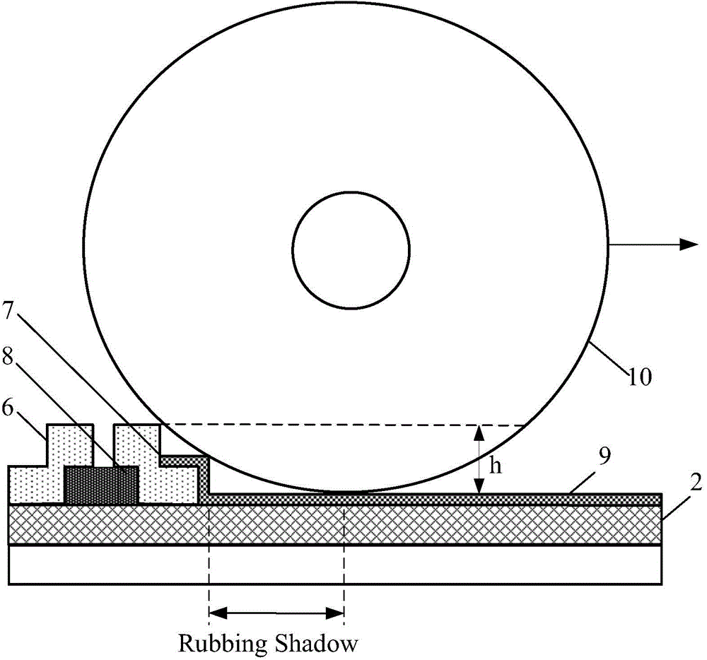
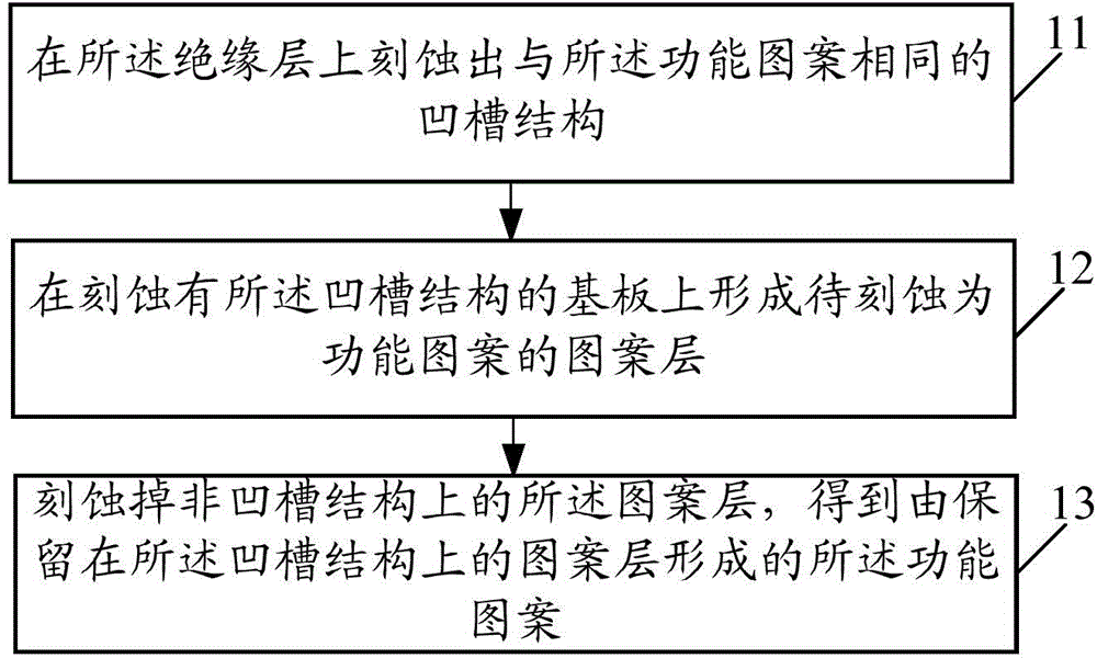
[0029] In the TFT array substrate manufactured by the traditional process, there is a large level difference near the edge of the pixel area, so when rubbing the alignment film on the pixel area, there will be a blind area. In order to solve this problem, the present invention provides a new pattern making method, which can effectively improve the flatness between the thin film transistor region and the pixel region, such as figure 2 As shown, the method of the present embodiment includes:

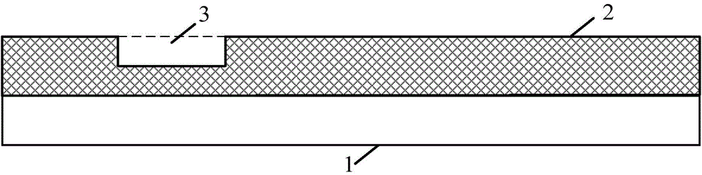
[0030] Step 21, etching a groove structure identical to the functional pattern on the insulating layer; the thickness of the groove structure is smaller than the thickness of the insulating layer;

[0031] Step 22, forming a pattern layer to be etched into a functi...


PUM


Abstract

The invention provides a graph production method, an array substrate and a display device, and relates to the display field. The graph production method includes: etching a groove structure as same as a function pattern on an insulating layer, wherein the thickness of the groove structure is less than the thickness of the insulating layer; forming a pattern layer to be etched into the function pattern on a base plate with the etched groove structure; etching all portions of the pattern layer, not located on the groove structure, so as to obtain the function pattern formed by the other portion of the pattern layer, retained on the groove structure. The graph production method, the array substrate and the display device can effectively reduce the number of bulges of the function pattern formed on the insulating layer, flat portions of the insulating layer, nearby edges of pixel regions, and thereby improve a rubbing technology of PI (polyimide) films, and prevent a light leakage phenomenon from occurring.

Description

technical field [0001] The invention relates to the field of display, in particular to a pattern making method, an array substrate and a display device. Background technique [0002] A liquid crystal display device includes an array substrate, a color filter substrate, and liquid crystals arranged between the array substrate and the color filter substrate. In order to stabilize the orientation of the liquid crystal on the array substrate and the color filter substrate without applying voltage, it is necessary to arrange a PI (Polyimide, polyimide) film on the array substrate. [0003] figure 1 It is a schematic diagram of rubbing a PI thin film on a TFT substrate (taking the top gate structure as an example). It can be seen from the figure that the source electrode 6, the drain electrode 7, and the semiconductor layer pattern 8 above the insulating layer all have protrusions. Therefore, there will be a level difference h near the edge of the pixel area 9, and when the roll...

Claims


Application Information

Patent Timeline
IPC IPC(8): H01L21/77H01L27/12G02F1/1337
CPCH01L21/77H01L27/1222H01L27/1259H01L27/127H01L2021/775
Inventor 苗青吴俊
Owner BOE TECH GRP CO LTD
Features
  • R&D
  • Intellectual Property
  • Life Sciences
  • Materials
  • Tech Scout
  • Unparalleled Data Quality
  • Higher Quality Content
  • 60% Fewer Hallucinations
Learn More