Packaging structure and packaging method for fingerprint identification module

A fingerprint recognition module and fingerprint recognition technology, which is applied in character and pattern recognition, instruments, electrical components, etc., can solve the problems of low sensitivity and recognition efficiency, high cost, and poor compression resistance of fingerprint recognition modules, so as to improve sensitivity and recognition efficiency, increase resistance to oppression, and reduce the effect of distance

Active Publication Date: 2015-05-20
NAT CENT FOR ADVANCED PACKAGING
View PDF8 Cites 11 Cited by
  • Summary
  • Abstract
  • Description
  • Claims
  • Application Information

AI Technical Summary

Problems solved by technology

[0005] In view of this, the embodiment of the present invention provides a packaging structure and packaging method of a fingerprint recognition module t

Method used


Image

  • Packaging structure and packaging method for fingerprint identification module
  • Packaging structure and packaging method for fingerprint identification module
  • Packaging structure and packaging method for fingerprint identification module

Examples


Example Embodiment

[0047] The present invention will be further described in detail below with reference to the drawings and embodiments. It can be understood that the specific embodiments described here are only used to explain the present invention, but not to limit the present invention. In addition, it should be noted that, for ease of description, the drawings only show part but not all of the content related to the present invention, and the size and size of the structure shown in the drawings are not actual or in proportion to the actual The size of the structure.

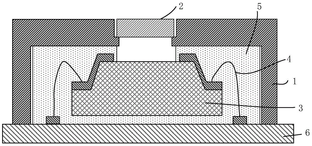
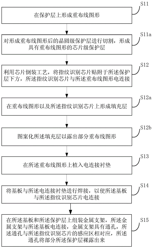
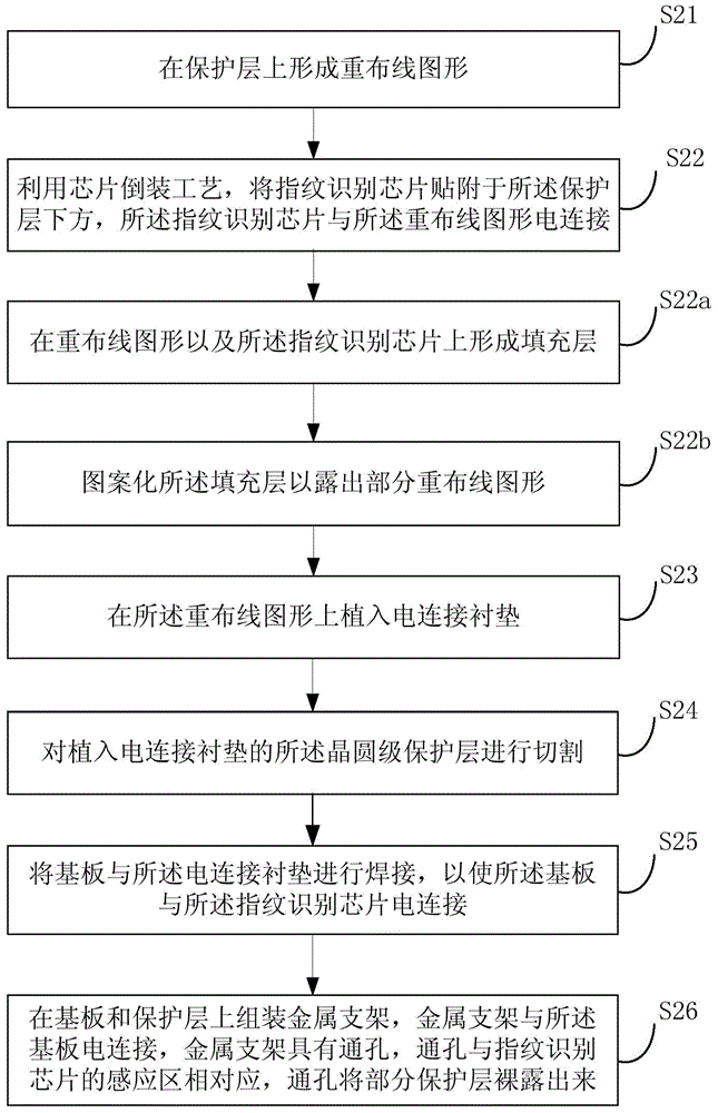
[0048] figure 2 It is a flowchart of a packaging method for a fingerprint identification module provided by an embodiment of the present invention. The fingerprint identification module encapsulated by this method can be applied to mobile terminals such as mobile phones, tablets, laptops, or media players, or Used in financial terminal equipment such as ATM machines. Such as figure 2 As shown, the packaging method of the fing...


PUM


Abstract

The invention discloses a packaging structure and a packaging method for a fingerprint identification module. The packaging method comprises the following steps: forming a wire re-arrangement graph on a protection layer; attaching a fingerprint identification chip below the protection layer by a chip inversion technology, wherein the fingerprint identification chip is electrically connected with the wire re-arrangement graph; implanting an electric connection liner into the wire re-arrangement graph; welding a substrate with the electric connection liner to enable the substrate to be electrically connected with the fingerprint identification chip; assembling a metal bracket on the substrate and the protection layer, wherein the metal bracket is electrically connected with the substrate and is provided with a through hole; the through hole corresponds to an induction region of the fingerprint identification chip and is used for exposing part of the protection layer. According to the packaging method, a distance between the contact surface of a fingerprint and the induction region of the fingerprint identification chip is reduced, and the identification efficiency is improved; furthermore, no welding wire is needed; the stress resistance of electric connection of the fingerprint identification module is improved.

Description

technical field [0001] The invention relates to the field of semiconductor device manufacturing, in particular to a packaging method of a fingerprint recognition module and a packaging structure of the fingerprint recognition module. Background technique [0002] Due to the lifelong invariance, uniqueness and convenience of fingerprints, the fingerprint identification system can process the collected fingerprints and perform identity authentication quickly and accurately. [0003] First, the fingerprint image is collected by the fingerprint identification module, and then the collected fingerprint image is input into the fingerprint identification system for identification and processing. Therefore, the quality of the fingerprint image will directly affect the accuracy of identification and the processing speed of the fingerprint identification system. Therefore, The fingerprint identification module is one of the key components in the fingerprint identification system. [...

Claims


Application Information

Patent Timeline
IPC IPC(8): H01L23/31G06K9/00
CPCH01L2224/48091H01L2924/00014
Inventor 张春艳
Owner NAT CENT FOR ADVANCED PACKAGING
Why Eureka
Try Eureka